SNOSD26 May 2016 TLV521
PRODUCTION DATA.
- 1 Features
- 2 Applications
- 3 Description
- 4 Revision History
- 5 Pin Configuration and Functions
- 6 Specifications
- 7 Detailed Description
- 8 Applications and Implementation
- 9 Power Supply Recommendations
- 10Layout
- 11Device and Documentation Support
- 12Mechanical, Packaging, and Orderable Information
Package Options
Mechanical Data (Package|Pins)
- DCK|5
Thermal pad, mechanical data (Package|Pins)
Orderable Information
1 Features
- Unmatched Price Performance
- For VS = 3.3 V, Typical Unless Otherwise Noted
- Ultra-low Supply Current
- 350 nA Typical, 500 nA Maximum
- Wide Operating Voltage Range 1.7 V to 5.5 V
- Low TCVOS 1.5 µV/°C
- VOS 3 mV (Max)
- Input Bias Current 1 pA
- PSRR 100 dB
- CMRR 90 dB
- Open-Loop Gain 110 dB
- Gain Bandwidth Product 6 kHz
- Slew Rate 2.5 V/ms
- Input Voltage Noise at f = 100 Hz 300 nV/√Hz
- Temperature Range –40ºC to 125°C
- Rail to Rail Input and Output (RRIO)
- Ultra-low Supply Current
2 Applications
- Wireless Remote Sensors
- Powerline Monitoring
- Power Meters
- Battery Powered Industrial Sensors
- Micropower Oxygen Sensor and Toxic Gas Sensor
- Active RFID Readers
- Zigbee Based Sensors for HVAC Control
- Sensor Network Powered by Energy Scavenging
- Current Sensing
- Glucose Monitoring
3 Description
The TLV521 350 nA nanopower op amp offers optimum price performance in TI's nanopower family of operational amplifiers. The TLV521 has a carefully designed CMOS input stage enabling very low Ibias of 1 pA, thereby reducing IBIAS and IOS errors that would otherwise impact sensitive applications like Megaohm resistance, high-impedance photodiode and charge sense situations. Additionally, built-in EMI protection reduces sensitivity to unwanted RF signals from sources like mobile phones and RFID readers.
The TLV521 is offered in the 5-pin SC70 package, and operates from –40°C to 125°C.
Device Information(1)
| PART NUMBER | PACKAGE | BODY SIZE (NOM) |
|---|---|---|
| TLV521 | SC70 (5) | 2.00 mm x 1.25 mm |
- For all available packages, see the orderable addendum at the end of the data sheet.
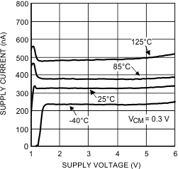
Nanopower Supply Current
