SLVSDJ7B May 2016 – August 2017 TPS564201
PRODUCTION DATA.
- 1 Features
- 2 Applications
- 3 Description
- 4 Revision History
- 5 Pin Configuration and Functions
- 6 Specifications
- 7 Detailed Description
- 8 Application and Implementation
- 9 Power Supply Recommendations
- 10Layout
- 11Device and Documentation Support
- 12Mechanical, Packaging, and Orderable Information
Package Options
Mechanical Data (Package|Pins)
- DDC|6
Thermal pad, mechanical data (Package|Pins)
Orderable Information
1 Features
- TPS564201 4-A Converter Integrated 50-mΩ and 22-mΩ FETs
- D-CAP2™ Mode Control with Fast Transient Response
- Input Voltage Range: 4.5 V to 17 V
- Output Voltage Range: 0.76 V to 7 V
- Pulse Skip Mode
- 560-kHz Switching Frequency
- Low Shutdown Current Less than 5 µA
- 1.6% Feedback Voltage Accuracy (25ºC)
- Startup from Pre-Biased Output Voltage
- Cycle-by-Cycle Overcurrent Limit
- Hiccup-mode Overcurrent Protection
- Non-Latch UVP and TSD Protections
- Fixed Soft Start: 1.0 ms
- Create a Custom Design Using the TPS564201 With the WEBENCH® Power Designer
2 Applications
- Digital TV Power Supply
- High Definition Blu-ray™ Disc Players
- Networking Home Terminal
- Digital Set Top Box (STB)
- Surveillance
3 Description
The TPS564201 is a simple, easy-to-use, 4-A synchronous step-down converter in SOT-23 package.
The device is optimized to operate with minimum external component count and also optimized to achieve low standby current.
These switch mode power supply (SMPS) devices employ D-CAP2 mode control providing a fast transient response and supporting both low-equivalent series resistance (ESR) output capacitors such as specialty polymer and ultra-low ESR ceramic capacitors with no external compensation components.
The TPS564201 operates in pulse skip mode, maintaining high efficiency during light load operation. The TPS564201 is available in a 6-pin 1.6-mm × 2.9-mm SOT (DDC) package, and specified from a –40°C to 125°C junction temperature.
Device Information(1)
| PART NUMBER | PACKAGE | BODY SIZE (NOM) |
|---|---|---|
| TPS564201 | DDC (6) | 1.60 mm × 2.90 mm |
- For all available packages, see the orderable addendum at the end of the data sheet.
space
space
space
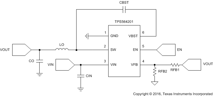
Simplified Schematic

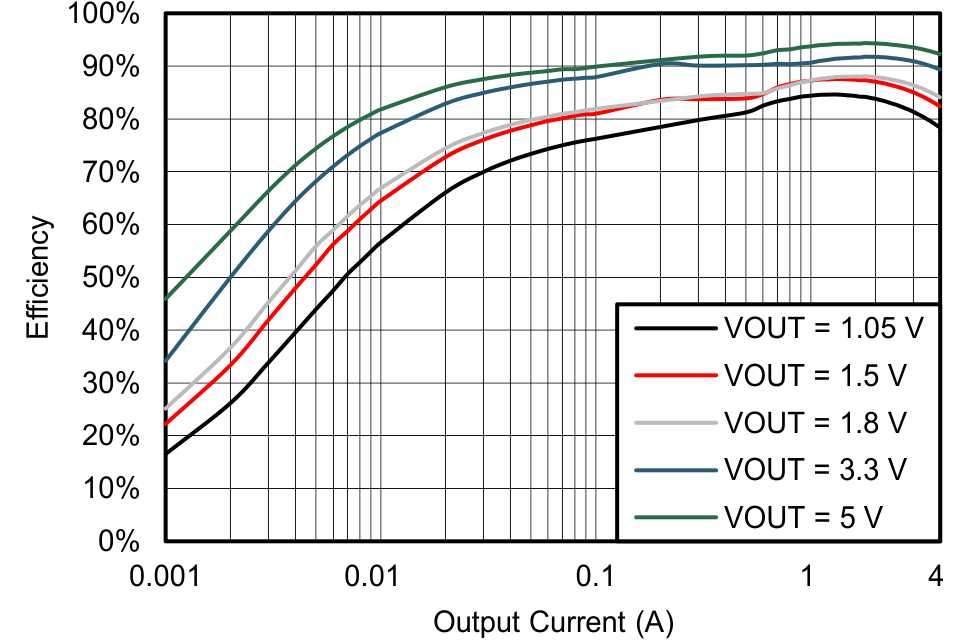
TPS564201 Efficiency
