SLLSEO3 July 2015 SN65HVD63
PRODUCTION DATA.
- 1 Features
- 2 Applications
- 3 Description
- 4 Revision History
- 5 Device Comparison Table
- 6 Pin Configuration and Functions
- 7 Specifications
- 8 Parameter Measurement Information
- 9 Detailed Description
- 10Application and Implementation
- 11Power Supply Recommendations
- 12Layout
- 13Device and Documentation Support
- 14Mechanical, Packaging, and Orderable Information
パッケージ・オプション
メカニカル・データ(パッケージ|ピン)
- RGT|16
サーマルパッド・メカニカル・データ
- RGT|16
発注情報
1 Features
- 3-V to 5.5-V Supply Range
- 1.6-V to 5.5-V Independent Logic Supply
- –15-dBm to +5-dBm Wide-Input Dynamic Range
for Receiver - 0-dBm to 6-dBm Adjustable Power
Delivered by the Driver to the Coax - AISG® V2.0-Compliant Output Emission Profile
Also Conforms to Proposed AISG V3.0 Specifications - Low-Power Standby Mode
- Direction Control Output
for RS-485 Bus Arbitration - Up to 115 kbps of Signaling Support
- 2.176-MHz Center Frequency
for Integrated Active Bandpass Filter - 3-mm × 3-mm 16-Pin VQFN Package
2 Applications
- AISG – Interface for Antenna Line Devices
- Tower-Mounted Amplifiers (TMA)
- General Modem Interfaces
3 Description
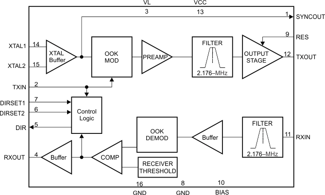
The SN65HVD63 transceiver modulates and demodulates signals between a logic (baseband) interface and a frequency suitable for long coaxial media, to facilitate wired data transfer among radio equipment.
The SN65HVD63 device is an integrated AISG transceiver designed to meet the requirements of the upcoming Antenna Interface Standards Group v3.0 specification.
The SN65HVD63 receiver integrates an active bandpass filter to enable demodulation of signals even in the presence of spurious frequency components. The filter has a 2.176-MHz center frequency.
The transmitter supports adjustable output power levels from 0 dBm to 6 dBm delivered to the 50-Ω coax cable. The SN65HVD63 transmitter is compliant with the spectrum emission requirement provided by the AISG standard.
A direction control output facilitates bus arbitration for an RS-485 interface. This device integrates an oscillator input for a crystal, and also accepts standard clock inputs to the oscillator.
Device Information(1)
| PART NUMBER | PACKAGE | BODY SIZE (NOM) |
|---|---|---|
| SN65HVD63 | VQFN (16) | 3.00 mm × 3.00 mm |
- For all available packages, see the orderable addendum at the end of the data sheet.
Block Diagram
