SLVSBB2E May 2012 – March 2017 TPS65131-Q1
PRODUCTION DATA.
- 1 Features
- 2 Applications
- 3 Description
- 4 Revision History
- 5 Pin Configuration and Functions
- 6 Specifications
- 7 Parameter Measurement Information
- 8 Detailed Description
-
9 Application and Implementation
- 9.1 Application Information
- 9.2
Typical Applications
- 9.2.1
TPS65131-Q1 With VPOS = 10.5 V, VNEG = -10 V
- 9.2.1.1 Design Requirements
- 9.2.1.2 Detailed Design Procedure
- 9.2.1.3 Analog Supply Input Filter
- 9.2.1.4 Thermal Information
- 9.2.1.5 Application Curves
- 9.2.2 TPS65131-Q1 With VPOS = 5.5 V, VNEG = -5 V
- 9.2.3 TPS65131-Q1 With VPOS = 15 V, VNEG = -15 V
- 9.2.1
TPS65131-Q1 With VPOS = 10.5 V, VNEG = -10 V
- 10Power Supply Recommendations
- 11Layout
- 12Device and Documentation Support
- 13Mechanical, Packaging, and Orderable Information
パッケージ・オプション
メカニカル・データ(パッケージ|ピン)
- RGE|24
サーマルパッド・メカニカル・データ
- RGE|24
発注情報
1 Features
- Qualified for Automotive Applications
- AEC-Q100 Test Guidance With the Following Results:
- Dual Adjustable Output Voltages up to 15 V and down to –15 V
- 2–A Typical Switch-Current Limit for Boost and Inverter Main Switches
- High Conversion Efficiency
- Up to 91% at Positive Output Rail
- Up to 85% at Negative Output Rail
- Power-Save Mode at Low Load
- Independent Enable Inputs for Power-Up and Power-Down Sequencing
- Control Output for External PFET to Support Complete Supply Disconnect When Shut Down
- 2.7-V to 5.5-V Input-Voltage Range
- Minimum 1.25-MHz Fixed-Frequency PWM Operation
- Thermal Shutdown
- Overvoltage Protection on Both Outputs
- 0.2-µA Typical Shutdown Current
- Small 4-mm × 4-mm QFN-24 Package (RGE)
3 Description
The TPS65131-Q1 device is dual-output dc-dc converter generating a positive output voltage up to 15 V and a negative output voltage down to –15 V with output currents of typically 200 mA, depending on input-voltage to output-voltage ratio. With a total efficiency up to 85%, the device is ideal for portable battery-powered equipment. The input-voltage range of 2.7 V to 5.5 V allows, for example, 3.3-V and 5-V rails to power the TPS65131-Q1 device. The TPS65131-Q1 device comes in a QFN-24 package with thermal pad. Requiring few and small external components, the overall solution size can be small.
The converter operates with a fixed-frequency PWM control topology and, with power-save mode enabled, uses a pulse-skipping mode at light load currents. In operation, the typical overall device quiescent current is only 500 µA. In shutdown, the device draws typically 0.2 µA. Independent enable pins allow power-up and power-down sequencing for both outputs. The device has an internal current limit, overvoltage protection, and a thermal shutdown for highest reliability under fault conditions.
The TPS65131-Q1 device is qualified for automotive applications, according to AEC-Q100 temperature grade 2. The electrical characteristics are tested over –40°C to 125°C device junction temperature. This, combined with lowest shutdown currents, small solution size, package with thermal pad, plus good efficiency and protection features, targets automotive and industrial applications.
Device Information(1)
| PART NUMBER | PACKAGE | BODY SIZE (NOM) |
|---|---|---|
| TPS65131-Q1 | VQFN (24) | 4 mm × 4 mm |
- For all available packages, see the orderable addendum.
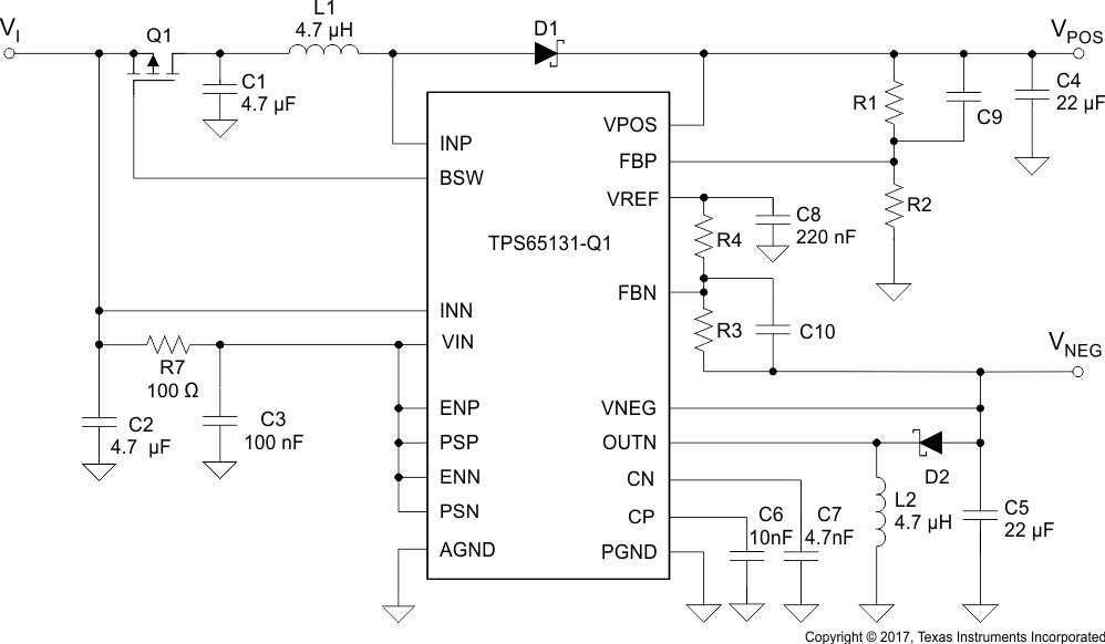
Application Schematic
