SBAS558C December 2012 – December 2015 ADS42B49
PRODUCTION DATA.
- 1 Features
- 2 Applications
- 3 Description
- 4 Revision History
- 5 Description (continued)
- 6 ADS424x and ADS422x Family Comparison
- 7 Pin Configuration and Functions
-
8 Specifications
- 8.1 Absolute Maximum Ratings
- 8.2 ESD Ratings
- 8.3 Recommended Operating Conditions
- 8.4 Thermal Information
- 8.5 Electrical Characteristics: ADS42B49 (250 MSPS)
- 8.6 Electrical Characteristics: General
- 8.7 Digital Characteristics
- 8.8 Timing Requirements: LVDS and CMOS Modes
- 8.9 Serial Interface Timing Characteristics
- 8.10 Reset Timing (Only When Serial Interface is Used)
- 8.11 LVDS Timings at Lower Sampling Frequencies
- 8.12 CMOS Timings at Lower Sampling Frequencies
- 8.13 Typical Characteristics
- 9 Parameter Measurement Information
- 10Detailed Description
- 11Application and Implementation
- 12Power Supply Recommendations
- 13Layout
- 14Device and Documentation Support
- 15Mechanical, Packaging, and Orderable Information
パッケージ・オプション
メカニカル・データ(パッケージ|ピン)
- RGC|64
サーマルパッド・メカニカル・データ
- RGC|64
発注情報
1 Features
- Maximum Sample Rate: 250 MSPS
- Ultralow Power:
- 850-mW Total Power at 250 MSPS
- Integrated Analog Input Buffer:
- Input Capacitance: 2.2 pF at 170 MHz
- Input Resistance: 1.1 kΩ at 170 MHz
- High Dynamic Performance:
- 85-dBc SFDR at 170 MHz
- 70.7-dBFS SNR at 170 MHz
- Crosstalk: > 85 dB at 185 MHz
- Programmable Gain Up to 6 dB for
SNR and SFDR Trade-off - DC Offset Correction
- Output Interface Options:
- 1.8-V Parallel CMOS Interface
- Double Data Rate (DDR) LVDS with Programmable Swing:
- Standard Swing: 350 mV
- Low Swing: 200 mV
- Supports Low Input Clock Amplitude
Down to 200 mVPP - Package: 9.00 mm × 9.00 mm, 64-Pin Quad Flat No-Lead (VQFN) Package
2 Applications
3 Description
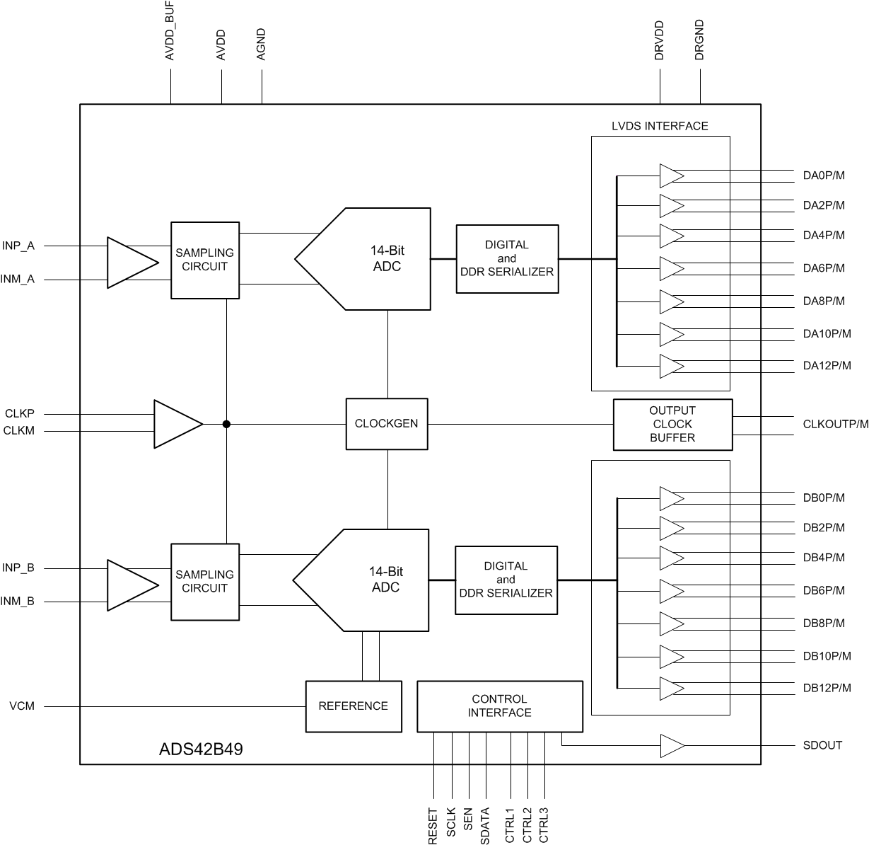
The ADS42B49 is an ultralow-power dual-channel, 14-bit analog-to-digital converter (ADC) featuring integrated analog input buffers. It uses innovative design techniques to achieve high dynamic performance, while consuming extremely low power. The presence of analog input buffers makes this device easy to drive and helps achieve high performance over a wide frequency range. The ADS42B49 is well-suited for multi-carrier, wide bandwidth communications applications.
Device Information(1)
| PART NUMBER | PACKAGE | BODY SIZE (NOM) |
|---|---|---|
| ADS42B49 | VQFN(64) | 9.00 mm × 9.00 mm |
- For all available packages, see the orderable addendum at the end of the data sheet.
Block Diagram
