SWRS283A June 2022 – November 2022 IWR6243
PRODUCTION DATA
- 1 Features
- 2 Applications
- 3 Description
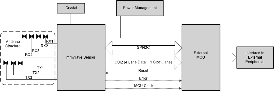
- 4 Functional Block Diagram
- 5 Revision History
- 6 Device Comparison
- 7 Terminal Configuration and Functions
-
8 Specifications
- 8.1 Absolute Maximum Ratings
- 8.2 ESD Ratings
- 8.3 Power-On Hours (POH)
- 8.4 Recommended Operating Conditions
- 8.5 Power Supply Specifications
- 8.6 Power Consumption Summary
- 8.7 RF Specification
- 8.8 Thermal Resistance Characteristics for FCBGA Package [ABL0161]
- 8.9
Timing and Switching Characteristics
- 8.9.1 Power Supply Sequencing and Reset Timing
- 8.9.2 Synchronized Frame Triggering
- 8.9.3 Input Clocks and Oscillators
- 8.9.4 Multibuffered / Standard Serial Peripheral Interface (MibSPI)
- 8.9.5 Inter-Integrated Circuit Interface (I2C)
- 8.9.6 LVDS Interface Configuration
- 8.9.7 General-Purpose Input/Output
- 8.9.8 Camera Serial Interface (CSI2)
- 9 Detailed Description
- 10Monitoring and Diagnostic Mechanisms
- 11Applications, Implementation, and Layout
- 12Device and Documentation Support
- 13Mechanical, Packaging, and Orderable Information
パッケージ・オプション
デバイスごとのパッケージ図は、PDF版データシートをご参照ください。
メカニカル・データ(パッケージ|ピン)
- ABL|161
サーマルパッド・メカニカル・データ
発注情報
1 Features
- FMCW transceiver
- Integrated PLL, transmitter, receiver, baseband, and ADC
- 57- to 64-GHz coverage with 7 GHz available bandwidth
- Four receive channels
- Three transmit channels
- Supports 6-bit phase shifter for TX Beam forming
- Ultra-accurate chirp engine based on Fractional-N PLL
- TX power: 12 dBm
- RX noise figure: 10 dB
- Phase noise at 1 MHz:
- –93dBc/Hz
- Built-in
calibration and self-test
- Self-calibrating system across process and temperature
- Host interface
- Control interface with external processor over SPI or I2C interface
- Data interface with external processor over MIPI D-PHY, CSI2 v1.1 and LVDS (only for debug)
- Interrupts for Fault Reporting
- Functional Safety-Compliant
- Developed for functional safety applications
- Documentation available to aid IEC 61508 functional safety system design up to SIL 3
- Hardware integrity up to SIL-2
- Safety-related certification
- IEC 61508 certified SIL-2 by TUV SUD
- IWR6243 Advanced features
- Embedded self-monitoring with limited Host processor involvement
- Complex baseband architecture
- Option of cascading multiple devices to increase channel count
- Embedded interference detection capability
- Power management
- Built-in LDO Network for enhanced PSRR
- I/Os support dual voltage 3.3 V/1.8 V
- Clock source
- Supports externally driven clock (square/sine) at 40 MHz
- Supports 40 MHz crystal connection with load capacitors
- Easy hardware
design
- 0.65-mm pitch, 161-pin 10.4 mm × 10.4 mm flip chip BGA package for easy assembly and low-cost PCB design
- Small solution size
- Operating Condtions :
- Junction temp range: –40°C to 105°C
 Figure 1-1 Radar Sensor
for Industrial Applications