SBOA325 May 2021 TLV9102 , TLV9152
Design Goals
| Input | Output | Supply | |||||
|---|---|---|---|---|---|---|---|
| ViMin | ViMax | IiMax | IoMin | IoMax | Vcc | Vee | Vload |
| 0V | 10V | 200µA | 0A | 1A | 15V | 0V | 36V |
Design Description
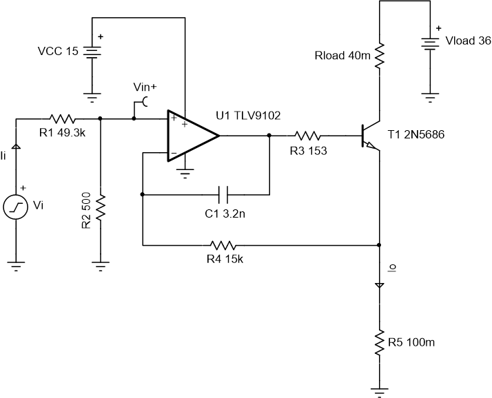
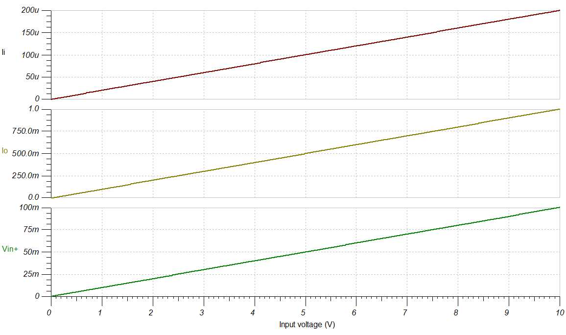
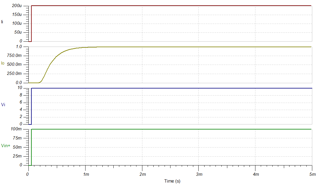
This low-side voltage-to-current (V-I) converter delivers a well-regulated current to a load which can be connected to a voltage greater than the op amp supply voltage. The circuit accepts an input voltage from 0V to 10V and converts it to a current from 0A and 1A. The current is accurately regulated by feeding back the voltage drop across a low-side current-sense resistor (R5) to the op amp.
Design Notes
- Resistor divider (R1 and R2) is implemented to limit the maximum voltage at the non-inverting input, Vin+, and sense resistor, R5, at full-scale.
- For an op amp that is not rail-to-rail input (RRI), a voltage divider may be needed to reduce the input voltage to be within the common-mode voltage of the op amp.
- Use low resistance values for R5 to maximize load compliance voltage and reduce the power dissipated at full-scale.
- Using a high-gain BJT reduces the output current requirement for the op amp.
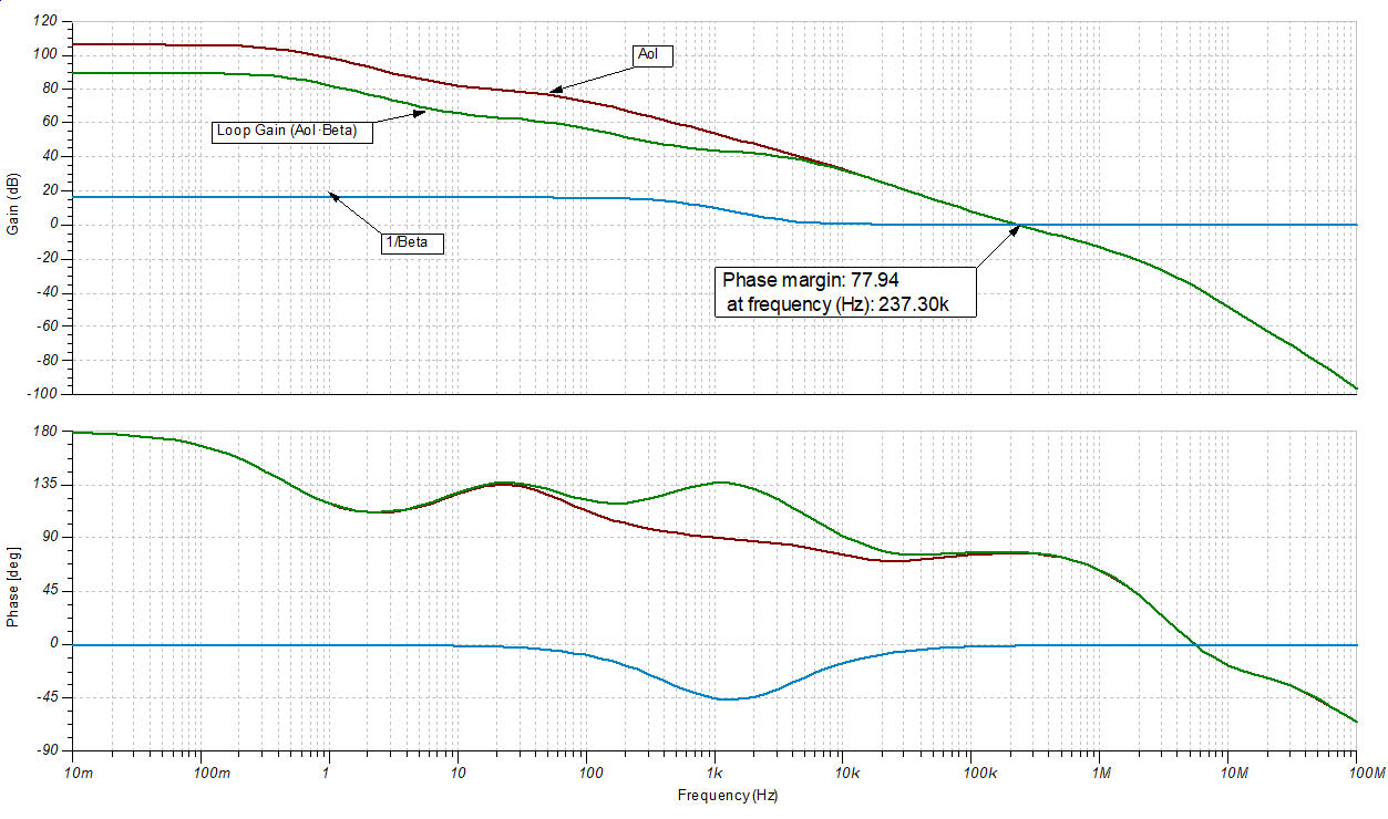
- Feedback components R3, R4, and C1 provide compensation to ensure stability. R3 isolates the input capacitance of the bipolar junction transistor (BJT), R4 provides a DC feedback path directly at the current-setting resistor (R5), and C1 provides a high-frequency feedback path that bypasses the BJT.
- Use the op amp in a linear operating region. Linear output swing is usually specified under the AOL test conditions in the device data sheet.
Design Steps
The transfer function of the circuit is:
- Calculate the sense resistor, R5. The sense resistor should be sized as small as possible to maximize the load compliance voltage and reduce power dissipation. Set the maximum voltage across the sense resistor to 100mV. Limiting the voltage drop to 100mV limits the power dissipated in the sense resistor to 100mW at full-scale output.
- Select resistors, R1 and R2, for the voltage divider at the input. At the maximum input voltage, the voltage divider should reduce the input voltage to the op amp, Vin+(max), to the maximum voltage across the sense resistor, R5. R1 and R2 should be chosen such that the maximum input current is not exceeded.
- See the Design References section [3] for the design procedure on how to properly size the compensation components, R3, R4, and C1.
Design Simulations
DC Simulation Results
AC Simulation Results
Transient Simulation Results
Design References
- See Analog Engineer's Circuit Cookbooks for TI's comprehensive circuit library.
- SPICE Simulation File: SBOMB58.
- TI Precision Labs
Design Featured Op Amp
| TLV9102 | |
|---|---|
| Vss | ±1.35V to ±8V, 2.7V to 16V |
| VinCM | Rail-to-rail |
| Vout | Rail-to-rail |
| Vos | 0.3mV |
| Iq | 120µA |
| Ib | 10pA |
| UGBW | 1.1MHz |
| SR | 4.5V/µs |
| #Channels | 1, 2, 4 |
| www.ti.com/product/TLV9102 | |
Design Alternate Op Amp
| TLV9152 | |
|---|---|
| Vss | ±1.35V to ±8V, 2.7V to 16V |
| VinCM | Rail-to-rail |
| Vout | Rail-to-rail |
| Vos | 125µV |
| Iq | 560µA |
| Ib | 10pA |
| UGBW | 4.5MHz |
| SR | 20V/µs |
| #Channels | 1, 2, 4 |
| www.ti.com/product/TLV9152 | |