SBOA515 April 2021 TLV1704-SEP
Design Goals
| Load Current (IL) | System Supply | Comparator Output Status | Radiation | |||
|---|---|---|---|---|---|---|
| Over Current (IOC) | Recovery Current (IRC) | Typical | Over Current | Normal Operation | Total Ionizing Dose (TID) | SEL Immunity to LET |
| 1 A | 0.5 A | 10 V | VOL < 0.4 V | VOH = VPU = 3.3 V | 30 krad(Si) | 43 MeV·cm2/mg |
Design Description
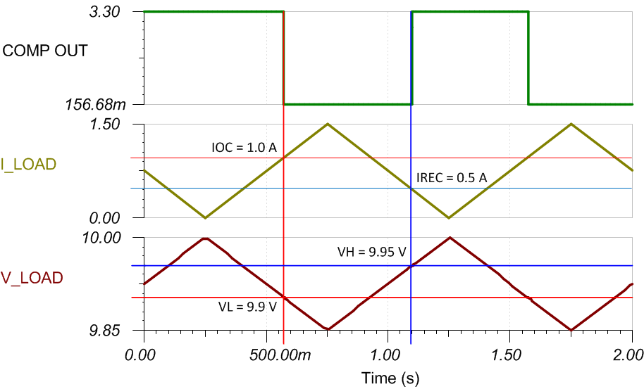
This application brief shows how to implement a simple rad-tolerant circuit that detects an over-current event caused by a single-event latch-up (SEL), in systems where not all other components SEL immune up to the target LET. This solution uses one comparator with a rail-to-rail input common mode range to create an over-current alert (OC-Alert) signal at the comparator output (COMP OUT) if the load current rises above 1A. The OC-Alert signal in this implementation is active low. So when the 1A threshold is exceeded, the comparator output goes low. Hysteresis is implemented such that OC-Alert will return to a logic high state when the load current reduces to 0.5A (a 50% reduction). This circuit uses an open-collector output comparator in order to level shift the output high logic level for controlling a digital logic input pin. For applications needing to drive the gate of a MOSFET switch, a comparator with a push-pull output is preferred.

Design Notes
- Select a comparator with rail-to-rail input common mode range to enable high-side current sensing.
- Select a comparator with an open-collector output stage for level-shifting.
- Select a comparator with low input offset voltage to optimize accuracy.
- Calculate the value for the shunt resistor (R6) so the shunt voltage (VSHUNT) is at least ten times larger than the comparator offset voltage (VIO).
Design Steps
- Select value of R6 so VSHUNT is at least 10x greater than the comparator input offset voltage (VIO). Note that making R6 very large will improve OC detection accuracy but will reduce supply headroom. Equation 1.Equation 1.
- Determine the desired switching thresholds for when the comparator output will transition from high-to-low (VL) and low-to-high (VH). VL represents the threshold when the load current crosses the OC level, while VH represents the threshold when the load current recovers to a normal operating level. Equation 1.Equation 1.
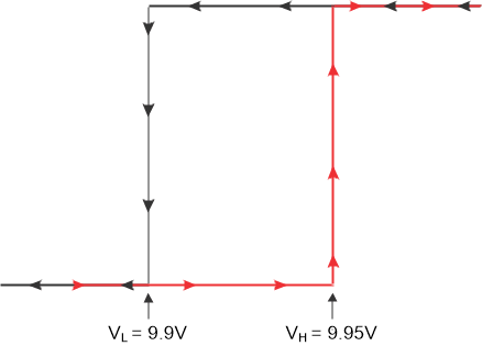
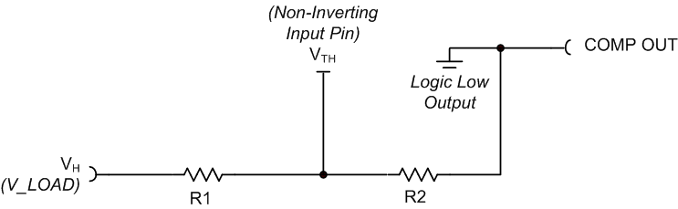
- With the non-inverting input pin of the comparator labeled as VTH and the comparator output in a logic low state (ground), derive an equation for VTH where VH represents the load voltage (VLOAD) when the comparator output transitions from low to high. Note that the simplified diagram for deriving the equation shows the comparator output as ground (logic low).
 Equation 1.
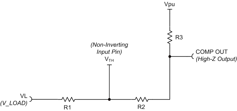
 - With the non-inverting input pin of the comparator labeled as VTH and the comparator output in a high-impedance state, derive an equation for VTH where VL represents the load voltage (VLOAD) when the comparator output transitions from high to low. Applying "superposition" theory to solve for VTH is recommended.
 Equation 1.
 - Eliminate variable VTH by setting the two equations equal to each other and solve for R1. The result is the following quadratic equation. Solving for R2 is less desirable since there are more standard values for small resistor values than the larger ones. Equation 1.
- Select values for R3 and R2. Please note that R3 is significantly smaller than R2 (R3<<R2). Increasing R3 will cause the comparator logic high output level to increase beyond VPU and should be avoided. For example, increasing R3 to a value of 100k can cause the logic high output to be 3.6 V. In this case, we can select R2 = 2M and R3 = 1k. Equation 1.Equation 1.
- Calculate R1 after substituting in numeric values for VPU, R2, VL, VH, and R3. For this design, set VPU = 3.3, R2 = 2M, VL = 9.9, VH = 9.95, and R3 = 1k. Equation 1.Equation 1.Equation 1.
- Calculate VTH using the equation derived in Design Step 3; use the calculated value for R1. Note that VTH is less than VL since VPU is less that VL. Equation 1.
- With the inverting terminal labeled as VTH, derive an equation for VTH in terms of R4, R5, and VS. Equation 1.
- Calculate R4 after substituting in numeric values R5=1M, VS=10, and the calculated value for VTH. Equation 1.Equation 1.
Design Simulations
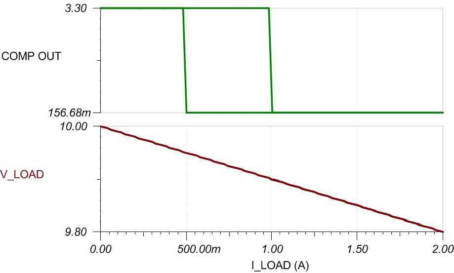
Transient Simulation Results
Design References
See Analog Engineer's Circuit Cookbooks for TI's comprehensive circuit library.
See Circuit SPICE Simulation File SBOMBL5, http://www.ti.com/lit/zip/sbombl5.
Design Featured Comparator
| TLV1704-SEP | |
|---|---|
| VS | 2.2 V to 36 V |
| VinCM | Rail-to-rail |
| VOUT | Open-Collector, Rail-to-rail |
| VOS | 500 µV |
| IQ | 55 µA/channel |
| tPD(HL) | 460 ns |
| #Channels | 4 |
TID Characterization (ELDRS-Free) | 30 krad(Si) |
TID Radiation Lot Acceptance Test (RLAT) / RHA | 20 krad(Si) |
SEL Immune to LET | 43 MeV·cm2/mg |
| https://www.ti.com/product/TLV1704-SEP | |