SLAAE92 January 2023 DAC43204 , DAC53004 , DAC53204 , DAC63004 , DAC63204
Design Objective
| Key Input Parameter | Key Output Signal | Recommended Device |
|---|---|---|
| SPI or I2C communication to set a programmable threshold, 0-V to 5.5-V analog input | Digital output of a comparator and data captured in NVM | DAC63204, DAC53204, DAC43204, DAC63004, DAC53004, DAC63202, DAC53202, DAC63002, DAC53002 |
Objective: Configure a smart DAC as a programmable comparator with hysteresis or a latching output, programmable window comparator, and save critical registers into NVM when a fault is detected.
Design Description
This circuit uses a four-channel buffered voltage-output DAC, such as the DAC63204, DAC53204, or DAC43204 (DACx3204), to create a comparator with a programmable threshold value. The DACx3204 has additional comparator features such as hysteresis, a latching output, or a window comparator mode. There is also a fault dump mode available which saves a few registers in the non-volatile memory (NVM) when the FAULT-DUMP bit in the register map is triggered or the general-purpose input/output (GPIO) pin, configured for fault dump mode, is triggered. This feature is useful in system-level fault management to capture the state of the device at the time the fault occurred. In this design, the integrated buffer acts as a comparator and the output of the DAC acts as the threshold for the comparator. The integrated buffer has an exposed feedback path via the feedback pin (FB) which acts as the voltage input to the comparator. All register settings are saved using the integrated non-volatile memory (NVM), enabling the device to be used without runtime software, even after a power cycle or reset. This circuit can be used in applications such as laser distance measurement, cordless vacuum cleaner, or medical accessories.
Design Notes
- The DACx3204 12-Bit, 10-Bit, and 8-Bit, Quad Voltage and Current Output Smart DACs With Auto-Detected I2C, PMBus™, or SPI Interface data sheet recommends using a 100-nF decoupling capacitor for the VDD pin and a 1.5-µF or greater bypass capacitor for the CAP pin. The CAP pin is connected to the internal LDO. Place these capacitors close to the device pins.
- Connect a 100-nF capacitor from VREF to GND if the external reference is used. Ramp up the external reference after VDD. Connect a pullup resistor from the VREF pin to VDD if the external reference is not used. This example uses VDD as the reference and the VREF pin is pulled up to VDD with a 10-kΩ resistor.
- Make sure the comparator input signal on the FBx pins does not exceed VDD. The maximum comparator threshold voltage is equal to the full-scale voltage of each DAC channel which is determined by the reference and gain settings of each channel. Larger input voltages can be scaled using a voltage divider and the threshold code can also be scaled accordingly.
- The FBx pins have a typical input impedance of 500 kΩ. Keep the series resistance of the input source low to avoid an offset error on the comparator input. This error can be compensated by adjusting the comparator threshold voltage by the offset voltage.
- Each DAC channel can be configured in a different comparator mode.
- Set the CMP-X-MODE bit in the DAC-X-CMP-MODE-CONFIG register to 0b00 for normal comparator mode. Enable each comparator channel by setting the CMP-X-EN bit in the respective DAC-X-VOUT-CMP-CONFIG register. To invert the comparator output, write 1 to the CMP-X-INV-EN bit. The FBx pins are a high-impedance input by default. Write 1 to the CMP-X-HIZ-IN-DIS bit to configure the FBx pins as finite-impedance inputs. The comparator output can be configured as push-pull or open-drain using the CMP-X-OD-EN bit. To enable the comparator output on the output pin, write 1 to the CMP-X-OUT-EN bit. Otherwise, read the comparator result in the CMP-FLAG-X bit of the CMP-STATUS register.
- Set the CMP-X-MODE bit in the DAC-X-CMP-MODE-CONFIG register to 0b01 to use hysteresis mode. The two hysteresis thresholds are set by the DAC codes in the DAC-X-MARGIN-HIGH and DAC-X-MARGIN-LOW registers. When the DAC-X-MARGIN-HIGH is set to full-code or the DAC-X-MARGIN-LOW is set to zero-code, the comparator works as an active low or active high latching comparator. The output is latched after the first threshold is crossed because the output is never able to cross the second full-code or zero-code output depending on the polarity. The latched output can be reset by writing to the corresponding RST-CMP-FLAG-X bit in the COMMON-DAC-TRIG register. Configure the remaining comparator settings in the DAC-X-VOUT-CMP-CONFIG register.
- Set the CMP-X-MODE bit in the DAC-X-CMP-MODE-CONFIG register to 0b10 to select window comparator mode. The window bounds are set by the DAC codes in the DAC-X-MARGIN-HIGH and the DAC-X-MARGIN-LOW registers. The status of the window comparator for a given channel is read from the respective WIN-CMP-X bit in the CMP-STATUS register. The static behavior of the WIN-CMP-X bit is not reflected on the output pins, so set the CMP-X-OUT-EN bit to 0. One of the window comparator outputs can be mapped as an output on the GPIO pin by configuring the GPO-CONFIG field in the GPIO-CONFIG register. Write a 1 to the WIN-LATCH bit in the COMMON-CONFIG register to configure WIN-CMP-X as a latching output. After being latched, the comparator output can be reset using the corresponding RST-CMP-FLAG-X bit in the COMMON-DAC-TRIG register. The input must be within the window bounds for the reset to take effect. Configure the remaining comparator settings in the DAC-X-VOUT-CMP-CONFIG register.
- The DAC63204 has a fault dump mode that saves a few registers into the NVM when the FAULT-DUMP bit is triggered via software in the COMMON-TRIGGER register, or the GPIO mapped to fault dump is triggered. This feature is useful in system-level fault management to capture the state of the device or system just before a fault is triggered to allow for diagnosis after the fault has occurred. Configure the GPIO as an input by setting the GPI-EN bit in the GPIO-CONFIG register to 1, and the GPO-EN bit to 0. Set the GPI-CONFIG field to 0b0010 to configure the fault dump sequence to be triggered on a falling edge on the GPIO pin.
- Using a 5-V reference and the 12-bit DAC63204, the LSB size, or step size between each code, is about 1.22 mV. Using a lower reference voltage decreases the LSB size and increases the resolution of the comparator threshold value. Using a smaller reference limits the upper limit of the threshold value, but as previously discussed, input voltages can be scaled down, if necessary.
- The DAC63204 can be programmed with the initial register settings described in the Register Settings section using I2C or SPI. Save the initial register settings in the NVM by writing a 1 to the NVM-PROG field of the COMMON-TRIGGER register. After programming the NVM, the device loads all registers with the values stored in the NVM after a reset or a power cycle.
Design Results
This schematic is used for the following simulation of the DAC63204. The OUT0 and FB0 signals are measured on an oscilloscope at the test points marked on the schematic.
Normal Programmable Comparator Results
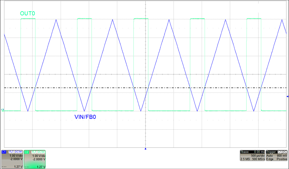
The 5-V VDD supply input is used as the reference and a 0-V to 5-V, 1-kHz triangle wave is applied to the input of the comparator (FB0 pin). The threshold value for the comparator is set to 1.25 V in the DAC-0-DATA register. The code programmed to these registers, in decimal, is calculated using:
The following plot shows the comparator output responding to the 1-kHz triangle wave on the FB0 pin. OUT0 changes as the triangle wave goes above or below the 1.25-V threshold set in the DAC-0-DATA register. The polarity of OUT0 can be reversed by setting the CMP-0-INV-EN bit to 1.
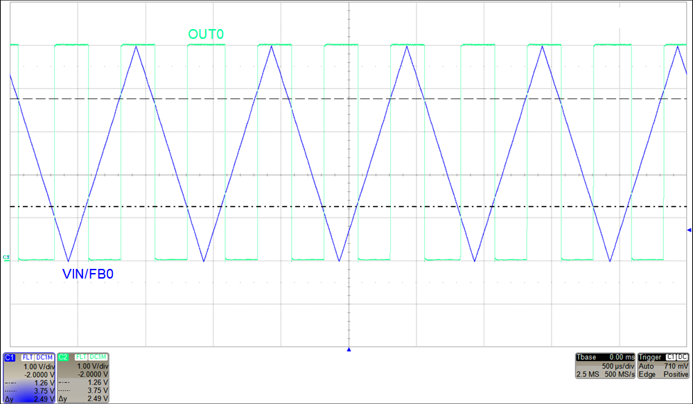
Programmable Comparator With Hysteresis Results
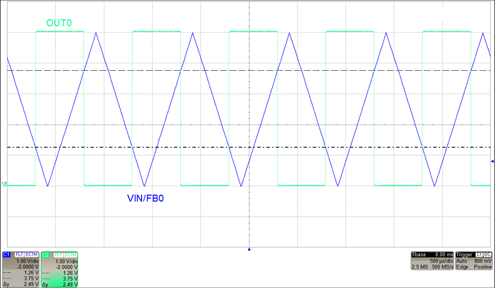
The 5-V VDD supply input is used as the reference and a 0-V to 5-V, 1-kHz triangle wave is applied to the input of the comparator (FB0 pin). The high threshold value for the comparator is set to 3.75 V in the DAC-0-MARGIN-HIGH register, and the low threshold is set to 1.25 V in the DAC-0-MARGIN-LOW register. The codes programmed to these registers, in decimal, are calculated using:
The following plot shows the comparator output responding to the 1-kHz triangle wave on the FB0 pin. OUT0 is high when the input goes above the 1.25-V threshold stored in DAC-0-MARGIN-LOW and is low when the input goes below the 3.75-V threshold stored in DAC-0-MARGIN-HIGH. The polarity of OUT0 can be reversed by setting the CMP-0-INV-EN bit to 1.
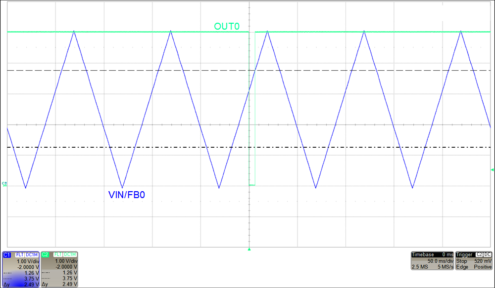
Active Low Latching Comparator Results
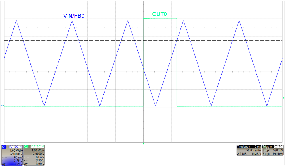
The 5-V VDD supply input is used as the reference and a 0-V to 5-V, 10-Hz triangle wave is applied to the input of the comparator (FB0 pin). The high threshold value for the comparator is set to 3.75 V in the DAC-0-MARGIN-HIGH register, and the low threshold is set to 0 V in the DAC-0-MARGIN-LOW register. The codes programmed to these registers, in decimal, are calculated using:
The following plot shows output responding to the 10-Hz triangle wave on the FB0 pin. The comparator output is reset right before the first rising edge of OUT0. The OUT0 value is latched low after the input is greater than the 3.75-V threshold stored in DAC-0-MARGIN-HIGH. The polarity of OUT0 can be reversed by setting the CMP-0-INV-EN bit to 1. Reset the comparator by writing 1 to the RST-CMP-FLAG-0 bit in the COMMON-DAC-TRIG register.
Active High Latching Comparator Results
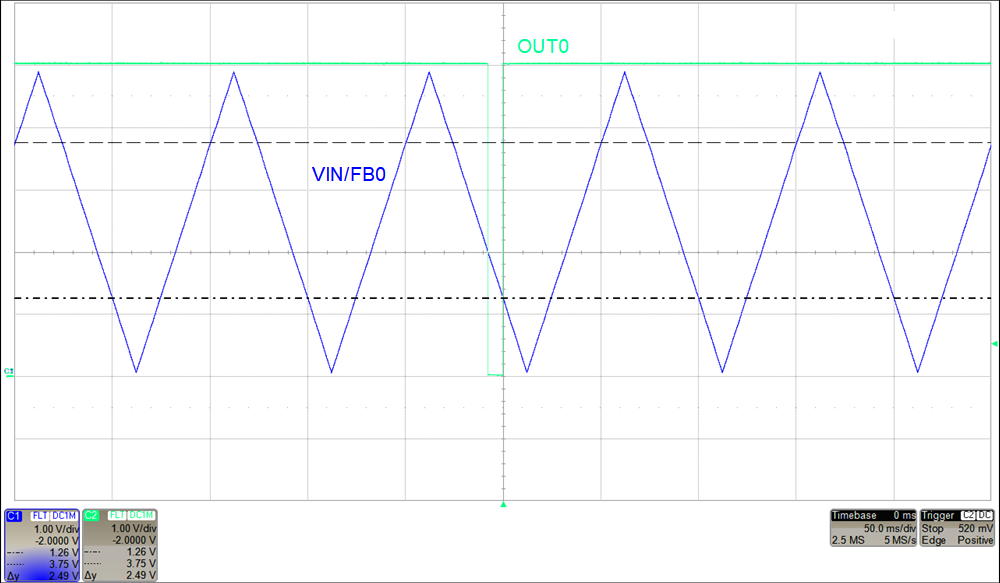
The 5-V VDD supply input is used as the reference and a 0-V to 5-V, 10-Hz triangle wave is applied to the input of the comparator (FB0 pin). The high threshold value for the comparator is set to 5 V in the DAC-0-MARGIN-HIGH register, and the low threshold is set to 1.25 V in the DAC-0-MARGIN-LOW register. The codes programmed to these registers, in decimal, are calculated using:
The following plot shows output responding to the 10-Hz triangle wave on the FB0 pin. The comparator output is reset right before the first falling edge of OUT0. The OUT0 value is latched high after the input is less than the 1.25-V threshold stored in DAC-0-MARGIN-LOW. The polarity of OUT0 can be reversed by setting the CMP-0-INV-EN bit to 1. Reset the comparator by writing 1 to the RST-CMP-FLAG-0 bit in the COMMON-DAC-TRIG register.
Programmable Window Comparator Results
The 5-V VDD supply input is used as the reference and a 0-V to 5-V, 1-kHz triangle wave is applied to the input of the comparator (FB0 pin). The high threshold value for the comparator is set to 3.75 V in the DAC-0-MARGIN-HIGH register, and the low threshold is set to 1.25 V in the DAC-0-MARGIN-LOW register. The GPIO pin is configured as an output and is mapped to WIN-CMP-0 by setting the GPO-CONFIG bit in the GPIO-CONFIG register to 0b1000. If using the DAC63204EVM board, remove jumper J6 so the GPIO pin is not connected to the EVM controller. The codes programmed to these registers, in decimal, are calculated using:
The following plot shows output responding to the 1-kHz triangle wave on the FB0 pin. The GPIO value mapped to WIN-CMP-0 is high when the input goes above the 3.75-V threshold stored in DAC-0-MARGIN-HIGH or below the 1.25-V threshold stored in DAC-0-MARGIN-LOW and is low when the input is within the window set by the two thresholds. The polarity of OUT0 can be reversed by setting the CMP-0-INV-EN bit to 1.
Programmable Window Comparator With Latching Output Results
The 5-V VDD supply input is used as the reference and a 0-V to 5-V, 1-kHz triangle wave is applied to the input of the comparator (FB0 pin). The high threshold value for the comparator is set to 3.75 V in the DAC-0-MARGIN-HIGH register, and the low threshold is set to 1.25 V in the DAC-0-MARGIN-LOW register. The GPIO pin is configured as an output and is mapped to WIN-CMP-0 output by setting the GPO-CONFIG bit in the GPIO-CONFIG register to 0b1000. If using the DAC63204EVM board, remove jumper J6 so the GPIO pin is not connected to the EVM controller. The codes programmed to these registers, in decimal, are calculated using:
This plot shows output responding to a 0-V to 5-V, 10-Hz triangle wave input on FB0 pin. The comparator output is reset right before the first falling edge of OUT0. The GPIO value mapped to WIN-CMP-0 is latched when the input is greater than the DAC-0-MARGIN-HIGH threshold level. The polarity of OUT0 can be reversed by setting the CMP-0-INV-EN bit to 1. Reset the comparator by writing 1 to the RST-CMP-FLAG-0 bit in the COMMON-DAC-TRIG register.
Fault Dump Results
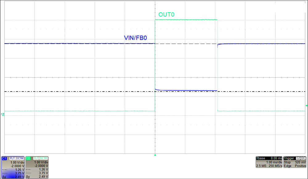
The 5-V VDD supply input is used as the reference. The input of the comparator (FB0 pin) is set to a step input from 3.75 V to 1.25 V. The threshold value for the comparator is set to 2.5 V in the DAC-0-DATA register. The OUT0 pin is connected to the GPIO pin which is configured as an input and mapped to trigger the fault dump sequence on a falling edge. Make sure the CMP-0-INV-EN bit is configured according to the polarity of the fault signal. If the fault dump needs to be triggered when the input is lower than the threshold, then set the CMP-0-INV-EN bit to 1. If the fault dump needs to be triggered when the input is higher than the threshold, then set the CMP-0-INV-EN bit to 0.
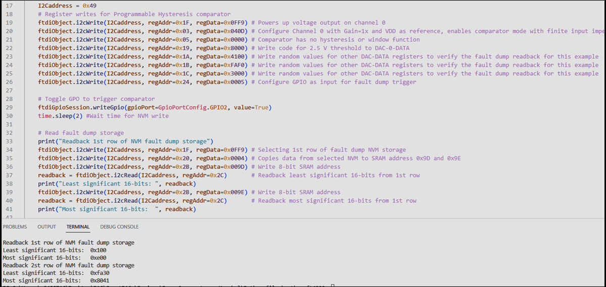
The data captured in the NVM after the fault dump can be read by following this sequence:
| NVM ROWS | B31–B24 | B23–B16 | B15–B8 | B7–B0 |
|---|---|---|---|---|
| Row 1 | CMP-STATUS[7:0] | Don't care | ||
| Row 2 | DAC-0-DATA[15:8] | DAC-1-DATA[15:8] | DAC-2-DATA[15:8] | DAC-3-DATA[15:8] |
- Set the EE-READ-ADDR bit to 0b in the COMMON-CONFIG register, to select row 1 of the NVM.
- Trigger the read of the selected NVM row by writing 1 to the READ-ONE-TRIG in the COMMON-TRIGGER register. This copies the data from the selected NVM row to SRAM addresses 0x9D (least significant 16 bits from the NVM) and 0x9E (most significant 16 bits from the NVM).
- To read the SRAM data:
- Write 0x009D to the SRAM-CONFIG register.
- Read the least significant 16 bits from the SRAM-DATA register.
- Write 0x009E to the SRAM-CONFIG register.
- Read the most significant 16 bits from the SRAM-DATA register.
- Set the EE-READ-ADDR bit to 1 in the COMMON-CONFIG register to select row 2 of the NVM. Repeat steps 2 and 3.
The following figure shows the terminal window which shows the fault dump storage readback after the GPIO falling edge. The most significant 8 bits of each DAC register are read back in the 2nd row of the fault dump storage. Random DAC values were stored in channels 1–3 for this example. The comparator status bits are shown in the most significant bits of the 1st NVM row. The status for comparator 0 is low. See the full pseudocode sequence in the Fault Dump Pseudocode Example.
Register Settings
The following table shows an example register map for this application. The values given here are for the design choices made in the Programmable Window Comparator with Latching Output Results section.
| Register Address | Register Name | Setting | Description |
|---|---|---|---|
0x1F | COMMON-CONFIG | 0x8FF9 | [15] 0b1: Write 0b1 to set the window comparator output to a latching output |
| [14] 0b0: Device not locked | |||
| [13] 0b0: Fault-dump read enable at address 0x00 | |||
| [12] 0b1: Disables the internal reference | |||
| [11:10] 0b11: Powers-down VOUT3 | |||
| [9] 0b0: Powers-down IOUT3 | |||
| [8:7] 0b11: Powers-down VOUT2 | |||
| [6] 0b0: Powers-down IOUT2 | |||
| [5:4] 0b11: Powers-down VOUT1 | |||
| [3] 0b0: Powers-down IOUT1 | |||
| [2:1] 0b11: Powers-up VOUT0 | |||
| [0] 0b0: Powers-down IOUT0 | |||
0x24 | GPIO-CONFIG | 0x3000 | [15] 0b0: Glitch filter disabled for GP input |
| [14] 0b0: Don't care | |||
| [13] 0b1: Write 0b1 to enable output mode on GPIO pin | |||
| [12:9] 0b1000: Selects the WIN-CMP-0 function setting mapped to GPIO as output | |||
| [8:5] 0b0000: Disables GPI function on all channels | |||
| [4:1] 0b0000: Configures the function of the GPI | |||
| [0] 0b0: Disables input mode for GPIO pin | |||
0x20 | COMMON-TRIGGER | 0x0002 | [15:12] 0b0000: Write 0b0101 to unlock the device |
| [11:8] 0b0000: Write 0b1010 to trigger a POR reset | |||
| [7] 0b0: LDAC not triggered | |||
| [6] 0b0: DAC clear not triggered | |||
| [5] 0b0: Don't care | |||
| [4] 0b0: Fault-dump is not triggered | |||
| [3] 0b0: PROTECT function not triggered | |||
| [2] 0b0: Fault-dump read not triggered | |||
| [1] 0b1: Write 0b1 to store applicable register settings to the NVM | |||
| [0] 0b0: NVM reload not triggered. Write 0b1 to reload applicable registers with existing NVM settings | |||
0x03, 0x09, 0x0F, 0x15 | DAC-X-VOUT-CMP-CONFIG | 0x0405 | [15:13] 0b000: Don't care |
[12:10] 0b001: Selects VDD as reference with 1× gain | |||
[9:5] 0x00: Don't care | |||
[4] 0b0: Set OUTx pins as push-pull in comparator mode | |||
[4] 0b0: Set OUTx pins as push-pull in comparator mode | |||
[3] 0b0: Comparator output consumed internally | |||
[2] 0b1: FBx input has finite impedance | |||
[1] 0b0: Comparator output not inverted | |||
[0] 0b1: Enables comparator mode | |||
0x05, 0x0B, 0x11, 0x17 | DAC-X-CMP-MODE-CONFIG | 0x0800 | [15:12] 0x0: Don't care |
[11:10] 0b10: Comparator configured in window comparator mode | |||
[9:0]: 0x000: Don't care | |||
| 0x01, 0x07, 0x0D, 0x13 | DAC-X-MARGIN-HIGH | 0xC000 | [15:4] 0xC00: 12-bit data updates the MARGIN-HIGH code |
| [3:0] 0x0: Don't care | |||
| 0x02, 0x08, 0x0E, 0x14 | DAC-X-MARGIN-LOW | 0x4000 | [15:4] 0x400: 12-bit data updates the MARGIN-LOW code |
| [3:0] 0x0: Don't care | |||
0x21 | COMMON-DAC-TRIG | 0x8000 | [15] 0b1: Resets latching or window comparator on channel 0 |
[14] 0b0: Channel 0 margin low not triggered | |||
[13] 0b0: Channel 0 margin high not triggered | |||
[12] 0b0: Channel 0 function generator not triggered | |||
[11:9] 0x0: Channel 1 triggers not affected | |||
| [7:4] 0x0: Channel 2 triggers not affected | |||
| [3:0] 0x0: Channel 3 triggers not affected |
Programmable Normal Comparator Pseudocode Example
The following shows a pseudocode sequence to program the initial register values to the NVM of the DAC63204. The values given here are for the design choices made in the Normal Programmable Comparator Results section.
1: //SYNTAX: WRITE <REGISTER NAME (Hex code)>, <MSB DATA>, <LSB DATA>
2: //Powers up voltage output on channel 0
3: WRITE COMMON-CONFIG(0x1F), 0x0F, 0xF9
4: //Configure Channel 0 with Gain=1x and VDD as reference, enables comparator mode with finite input impedance, and enables comparator output on OUT0
5: WRITE DAC-0-VOUT-CMP-CONFIG(0x03), 0x04, 0x0D
6: //Comparator has no hysteresis or window function
7: WRITE DAC-0-CMP-MODE-CONFIG(0x05), 0x00, 0x00
8: //Write threshold to DAC-0-DATA
9: //With 16-bit left alignment 0x400 becomes 0x4000
10: WRITE DAC-0-Data(0x19), 0x40, 0x00
11: //Save settings to NVM
12: WRITE COMMON-TRIGGER(0x20), 0x00, 0x02
Programmable Comparator With Hysteresis Pseudocode Example
The following shows a pseudocode sequence to program the initial register values to the NVM of the DAC63204. The values given here are for the design choices made in the Programmable Comparator With Hysteresis Results section.
1: //SYNTAX: WRITE <REGISTER NAME (Hex code)>, <MSB DATA>, <LSB DATA>
2: //Powers up voltage output on channel 0
3: WRITE COMMON-CONFIG(0x1F), 0x0F, 0xF9
4: //Configure Channel 0 with Gain=1x and VDD as reference, enables comparator mode with finite input impedance, and enables comparator output on OUT0
5: WRITE DAC-0-VOUT-CMP-CONFIG(0x03), 0x04, 0x0D
6: //Configure comparator for hysteresis mode
7: WRITE DAC-0-CMP-MODE-CONFIG(0x05), 0x04, 0x00
8: //Write high threshold to DAC-0-MARGIN-HIGH
9: //With 16-bit left alignment 0xC00 becomes 0xC000
10: WRITE DAC-0-MARGIN-HIGH(0x01), 0xC0, 0x00
11: //Write low threshold to DAC-0-MARGIN-LOW
12: //With 16-bit left alignment 0x400 becomes 0x4000
13: WRITE DAC-0-MARGIN-LOW(0x02), 0x40, 0x00
14: //Save settings to NVM
15: WRITE COMMON-TRIGGER(0x20), 0x00, 0x02
Active Low Latching Comparator Pseudocode Example
The following shows a pseudocode sequence to program the initial register values to the NVM of the DAC63204. The values given here are for the design choices made in the Active Low Latching Comparator Results section.
1: //SYNTAX: WRITE <REGISTER NAME (Hex code)>, <MSB DATA>, <LSB DATA>
2: //Powers up voltage output on channel 0
3: WRITE COMMON-CONFIG(0x1F), 0x0F, 0xF9
4: //Configure Channel 0 with Gain=1x and VDD as reference, enables comparator mode with finite input impedance, and enables comparator output on OUT0
5: WRITE DAC-0-VOUT-CMP-CONFIG(0x03), 0x04, 0x0D
6: //Configure comparator for hysteresis mode
7: WRITE DAC-0-CMP-MODE-CONFIG(0x05), 0x04, 0x00
8: //Write high threshold to DAC-0-MARGIN-HIGH
9: //With 16-bit left alignment 0xC00 becomes 0xC000
10: WRITE DAC-0-MARGIN-HIGH(0x01), 0xC0, 0x00
11: //Write low threshold to DAC-0-MARGIN-LOW (set to zero-scale to latch)
12: WRITE DAC-0-MARGIN-LOW(0x02), 0x00, 0x00
13: //Save settings to NVM
14: WRITE COMMON-TRIGGER(0x20), 0x00, 0x02
15:
16: //Resets latching comparator output
17: WRITE COMMON-DAC-TRIG(0x21), 0x80, 0x00
Active High Latching Comparator Pseudocode Example
The following shows a pseudocode sequence to program the initial register values to the NVM of the DAC63204. The values given here are for the design choices made in the Active High Latching Comparator Results section.
1: //SYNTAX: WRITE <REGISTER NAME (Hex code)>, <MSB DATA>, <LSB DATA>
2: //Powers up voltage output on channel 0
3: WRITE COMMON-CONFIG(0x1F), 0x0F, 0xF9
4: //Configure Channel 0 with Gain=1x and VDD as reference, enables comparator mode with finite input impedance, and enables comparator output on OUT0
5: WRITE DAC-0-VOUT-CMP-CONFIG(0x03), 0x04, 0x0D
6: //Configure comparator for hysteresis mode
7: WRITE DAC-0-CMP-MODE-CONFIG(0x05), 0x04, 0x00
8: //Write high threshold to DAC-0-MARGIN-HIGH (set to full-scale to latch)
9: //With 16-bit left alignment 0xFFF becomes 0xFFF0
10: WRITE DAC-0-MARGIN-HIGH(0x01), 0xFF, 0xF0
11: //Write low threshold to DAC-0-MARGIN-LOW
12: //With 16-bit left alignment 0x400 becomes 0x4000
13: WRITE DAC-0-MARGIN-LOW(0x02), 0x40, 0x00
14: //Save settings to NVM
15: WRITE COMMON-TRIGGER(0x20), 0x00, 0x02
16:
17: //Resets latching comparator output
18: WRITE COMMON-DAC-TRIG(0x21), 0x80, 0x00
Programmable Window Comparator Pseudocode Example
The following shows a pseudocode sequence to program the initial register values to the NVM of the DAC63204. The values provided are for the design choices made in the Programmable Window Comparator Results section.
1: //SYNTAX: WRITE <REGISTER NAME (Hex code)>, <MSB DATA>, <LSB DATA>
2: //Powers up voltage output on channel 0
3: WRITE COMMON-CONFIG(0x1F), 0x0F, 0xF9
4: //Configure Channel 0 with Gain=1x and VDD as reference, enables comparator mode with finite input impedance, and disables comparator output on OUT0
5: WRITE DAC-0-VOUT-CMP-CONFIG(0x03), 0x04, 0x05
6: //Configure comparator for window comparator mode
7: WRITE DAC-0-CMP-MODE-CONFIG(0x05), 0x08, 0x00
8: //Write high threshold to DAC-0-MARGIN-HIGH
9: //With 16-bit left alignment 0xC00 becomes 0xC000
10: WRITE DAC-0-MARGIN-HIGH(0x01), 0xC0, 0x00
11: //Write low threshold to DAC-0-MARGIN-LOW
12: //With 16-bit left alignment 0x400 becomes 0x4000
13: WRITE DAC-0-MARGIN-LOW(0x02), 0x40, 0x00
14: //Configure GPIO as output for Channel 0 window comparator
15: WRITE GPIO-CONFIG(0x24), 0x30, 0x00
16: //Save settings to NVM
17: WRITE COMMON-TRIGGER(0x20), 0x00, 0x02
Programmable Window Comparator With Latching Output Pseudocode Example
The following shows a pseudocode sequence to program the initial register values to the NVM of the DAC63204. The values given here are for the design choices made in the Programmable Window Comparator with Latching Output Results section.
1: //SYNTAX: WRITE <REGISTER NAME (Hex code)>, <MSB DATA>, <LSB DATA>
2: //Powers up voltage output on channel 0, configures latching window comparator
3: WRITE COMMON-CONFIG(0x1F), 0x8F, 0xF9
4: //Configure Channel 0 with Gain=1x and VDD as reference, enables comparator mode with finite input impedance, and disables comparator output on OUT0
5: WRITE DAC-0-VOUT-CMP-CONFIG(0x03), 0x04, 0x05
6: //Configure comparator for window comparator mode
7: WRITE DAC-0-CMP-MODE-CONFIG(0x05), 0x08, 0x00
8: //Write high threshold to DAC-0-MARGIN-HIGH
9: //With 16-bit left alignment 0xC00 becomes 0xC000
10: WRITE DAC-0-MARGIN-HIGH(0x01), 0xC0, 0x00
11: //Write low threshold to DAC-0-MARGIN-LOW
12: //With 16-bit left alignment 0x400 becomes 0x4000
13: WRITE DAC-0-MARGIN-LOW(0x02), 0x40, 0x00
14: //Configure GPIO as output for Channel 0 window comparator
15: WRITE GPIO-CONFIG(0x24), 0x30, 0x00
16: //Save settings to NVM
17: WRITE COMMON-TRIGGER(0x20), 0x00, 0x02
18:
19: //Resets latching comparator output
20: WRITE COMMON-DAC-TRIG(0x21), 0x80, 0x00
Fault Dump Pseudocode Example
The following shows a pseudocode sequence to program the initial register values to the NVM of the DAC63204. The values given here are for the design choices made in the Fault Dump Results section.
1: //SYNTAX: WRITE <REGISTER NAME (Hex code)>, <MSB DATA>, <LSB DATA>
2: //Powers up voltage output on channel 0
3: WRITE COMMON-CONFIG(0x1F), 0x0F, 0xF9
4: //Configure Channel 0 with Gain=1x and VDD as reference, enables comparator mode with finite input impedance, and enables comparator output on OUT0
5: WRITE DAC-0-VOUT-CMP-CONFIG(0x03), 0x04, 0x0D
6: //Comparator has no hysteresis or window function
7: WRITE DAC-0-CMP-MODE-CONFIG(0x05), 0x00, 0x00
8: //Write code for 2.5 V threshold to DAC-0-DATA
9: //With 16-bit left alignment 0x800 becomes 0x8000
10: WRITE DAC-0-Data(0x19), 0x80, 0x00
11: //Write random values for other DAC-DATA registers to verify the fault dump readback for this example
12: WRITE DAC-1-Data(0x1A), 0x41, 0x00
13: WRITE DAC-2-Data(0x1B), 0xFA, 0xF0
14: WRITE DAC-3-Data(0x1C), 0x30, 0x00
15: //Configure GPIO as input for fault dump trigger
16: WRITE GPIO-CONFIG(0x24), 0x00, 0x05
17:
18: //Read fault dump storage
19: //Selecting 1st row of fault dump NVM storage
20: WRITE COMMON-CONFIG(0x1F), 0x0F, 0xF9
21 //Copies data from selected NVM to SRAM address 0x9D and 0x9E
22: WRITE COMMON-TRIGGER(0x20), 0x00, 0x04
23: //Write 8-bit SRAM address
24: WRITE SRAM-CONFIG(0x2B), 0x00, 0x9D
25: //Readback least significant 16-bits data from 1st row
26: READ SRAM-DATA (0x2B)
27: //Write 8-bit SRAM address
28: WRITE SRAM-CONFIG(0x2B), 0x00, 0x9E
29: //Readback most significant 16-bits data from 1st row
30: READ SRAM-DATA (0x2B)
31:
32: //Selecting 2nd row of fault dump NVM storage
33: WRITE COMMON-CONFIG(0x1F), 0x2F, 0xF9
34: //Copies data from selected NVM to SRAM address 0x9D and 0x9E
35: WRITE COMMON-TRIGGER(0x20), 0x00, 0x04
36: //Write 8-bit SRAM address
37: WRITE SRAM-CONFIG(0x2B), 0x00, 0x9D
38: //Readback least significant 16-bits data from 2nd row
39: READ SRAM-DATA (0x2B)
40: //Write 8-bit SRAM address
41: WRITE SRAM-CONFIG(0x2B), 0x00, 0x9E
42: //Readback ost significant 16-bits data from 2nd row
43: READ SRAM-DATA (0x2B)
Design Featured Devices
| Device | Key Features | Link |
|---|---|---|
| DAC63204 | 4-channel, 12-bit, VOUT and IOUT smart DAC with I2C, SPI and Hi-Z out during power off | DAC63204 |
| DAC53204 | 4-channel, 10-bit, VOUT and IOUT smart DAC with I2C, SPI and Hi-Z out during power off | DAC53204 |
| DAC43204 | 4-channel, 8-bit, VOUT and IOUT smart DAC with I2C, SPI and Hi-Z out during power off | DAC43204 |
| DAC63004 | 4-channel, ultra-low-power, 12-bit, VOUT and IOUT smart DAC with I2C, SPI and Hi-Z out during power off | DAC63004 |
| DAC53004 | 4-channel, ultra-low-power, 12-bit, VOUT and IOUT smart DAC with I2C, SPI and Hi-Z out during power off | DAC53004 |
| DAC63202 | 2-channel, 12-bit, VOUT and IOUT smart DAC with I2C, SPI and Hi-Z out during power off | DAC63202 |
| DAC53202 | 2-channel, 10-bit, VOUT and IOUT smart DAC with I2C, SPI and Hi-Z out during power off | DAC53202 |
| DAC63002 | 2-channel, ultra-low-power, 12-bit, VOUT and IOUT smart DAC with I2C, SPI and Hi-Z out during power off | DAC63002 |
| DAC53002 | 2-channel, ultra-low-power, 10-bit, VOUT and IOUT smart DAC with I2C, SPI and Hi-Z out during power off | DAC53002 |
Find other possible devices using the Parametric search tool.
Design References
See Analog Engineer's Circuit Cookbooks for TI's comprehensive circuit library.
Additional Resources
- Texas Instruments, DAC53701 Programmable Comparator With Hysteresis Simulation
- Texas Instruments, DAC63204 Evaluation Module
- Texas Instruments, DAC63204 EVM User’s Guide
- Texas Instruments, Precision Labs - DACs
For direct support from TI Engineers, use the E2E community: