SLVAEH7 October 2019 TPS66020 , TPS66021 , TPS66120 , TPS66121
1 TI Tech Note
Introduction
Texas Instruments offers a diverse portfolio of power switch products, also known as power multiplexers, for different power distribution applications, including USB Type-C/PD (Power Delivery). The product tree includes sink-only and sink/source switches with dead-battery LDO and OVP and RCP protection schemes.
This TI Tech Note provides layout guideline recommendations, permitting the use of non-HDI PCBs while benefitting from ultra-small 0.4-mm pitch WCSP packages.
Layout Guidelines
The 28-pin WSCP package used on the power switches described in this tech note have an optimized pin to function assignment and can be connected with the minimum numbers of metal layers. By following the layout guidelines described in coming sections, the user can use a non-HDI PCB process to save PCB cost.
TPS66120 Layout Guidelines
The TPS6612x contains an integrated 4-V to 22-V sink power path. The power path supports overtemperature and reverse current protection. VBUS has overvoltage protection with the level being set by an optional external resistor divider. If no overvoltage protection is desired, it may be disabled by grounding the OVP terminal.
The TPS6612x supports a fault pin that indicates over-temperature events. The TPS6612x series also supports a high-voltage VBUS LDO regulator, useful for supplying power to the device and other system components when operating in dead-battery conditions.
TPS66120 Pin Map
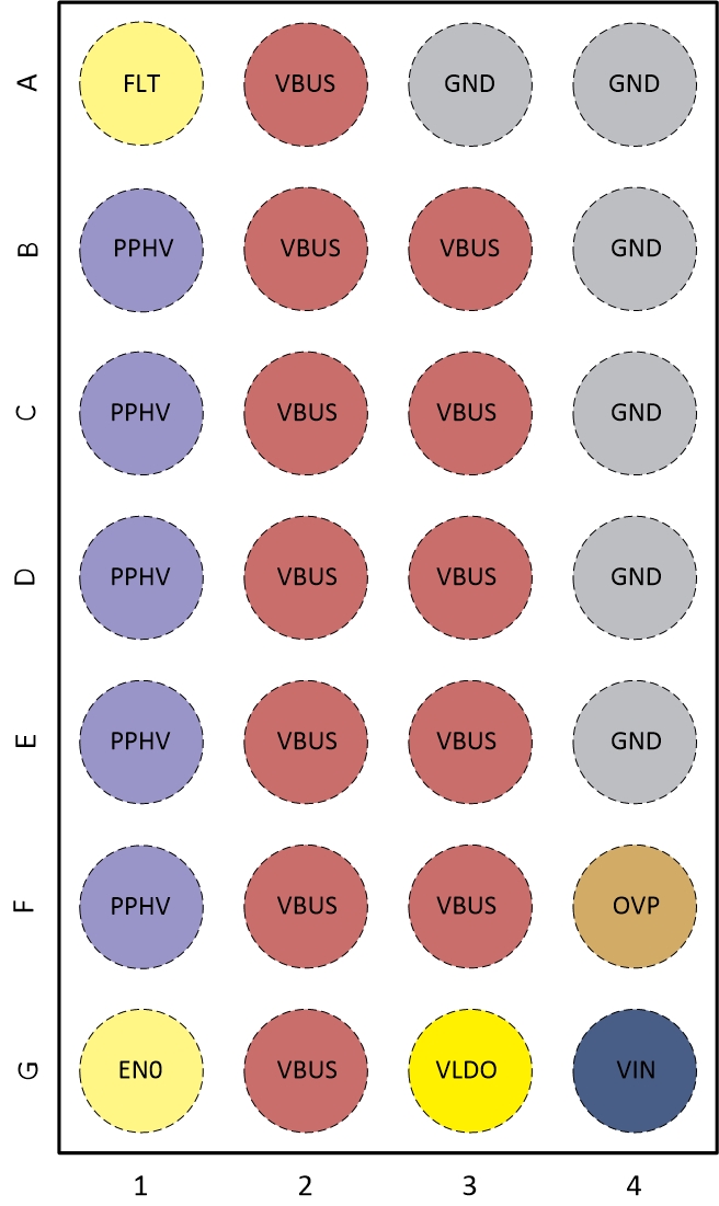
Figure 1 shows the top view of the TPS66120 Power switch multiplexer pin-to-function mapping.
 Figure 1. TPS66120 Pin Map
 TPS66120 Layout Guidelines
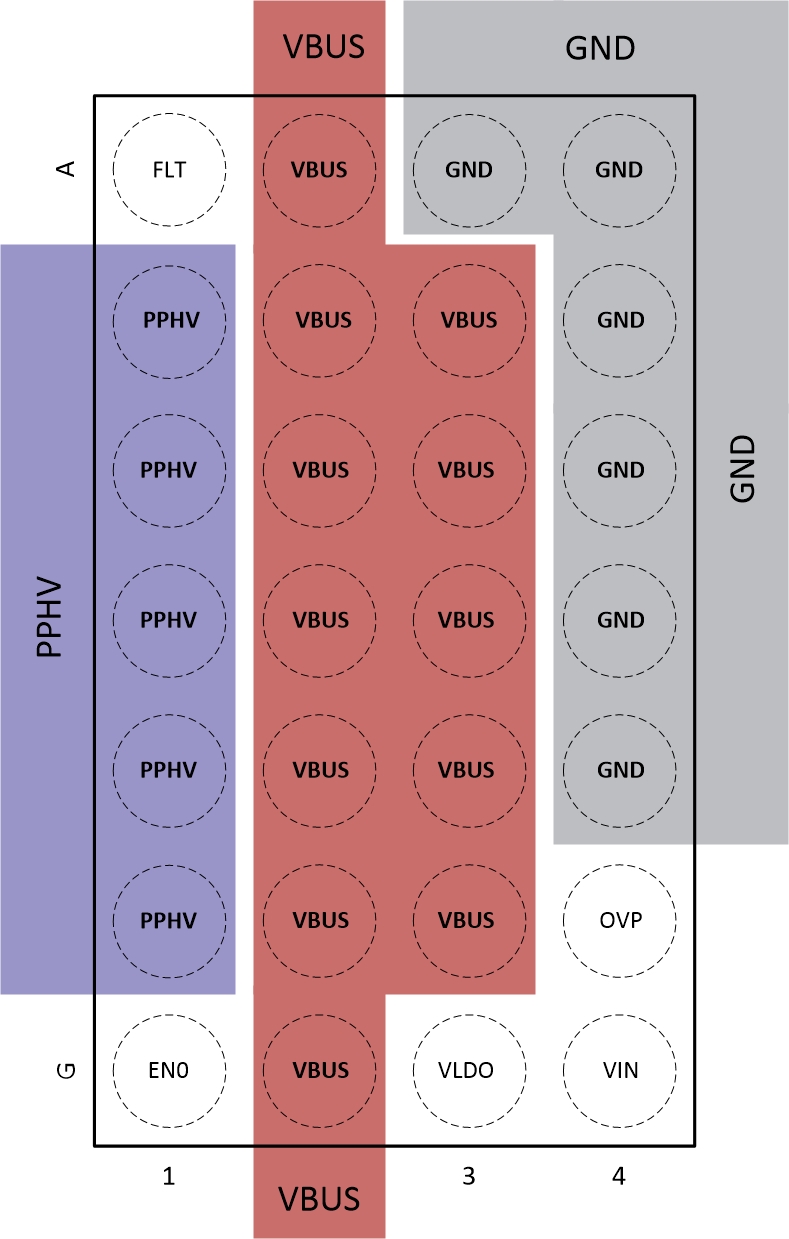
The layout guidelines shown in Figure 2 provide all the connections for power path, including VBUS, PPHV, GND, VIN, and VLDO. The signal pins are all at the edge of the ball array, therefore all of them can be connected out with one metal layer.
 Figure 2. TPS66120 Layout
 TPS66020 Layout Guidelines
The TPS66020 is a full-featured power switch multiplexer that contains an integrated 5-V source power path and a 4-V to 22-V sink power path. The 5-V Source path limits the output current to a safe level by operating in a constant-current mode when the output load exceeds the selected current-limit threshold.
Each power path supports overtemperature and reverse current protection. VBUS has overvoltage protection, with the level being set by an optional external resistor divider. If no overvoltage protection is desired, it may be disabled by grounding the OVP terminal. The TPS6602x series supports a fault pin that indicates overcurrent and overtemperature events.
TPS66020 Pin Map
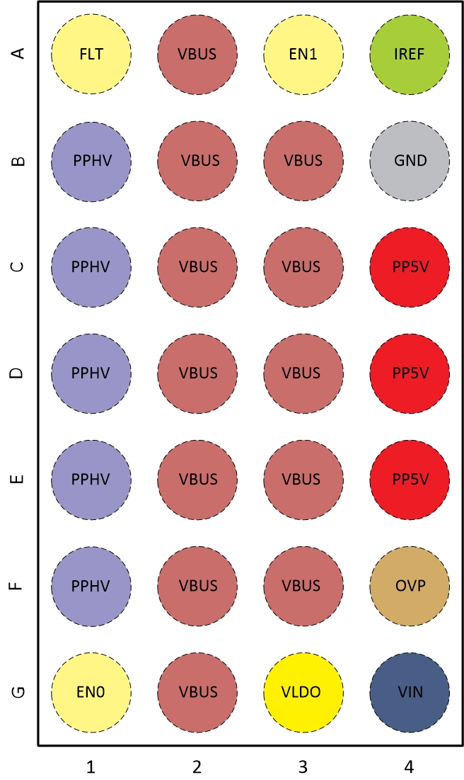
Figure 3 shows top view of the TPS66020 power switch multiplexer pin-to-function mapping.
 Figure 3. TPS66020 Pin Map
 TPS66020 Layout Guidelines
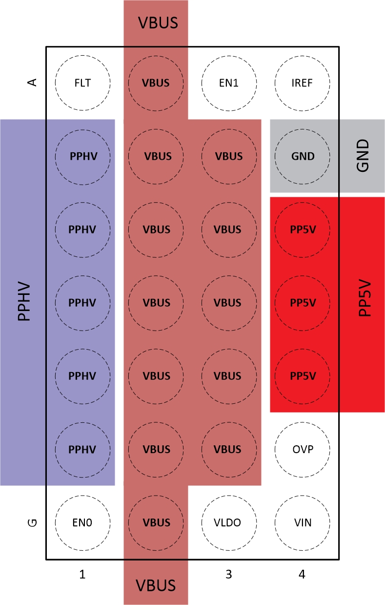
The layout guidelines shown in Figure 4 provide all the connections for power path, including VBUS, PPHV, PP5V, GND, VIN, and VLDO. The signal pins are all at the edge of the ball array, therefore all of them can be connected out with one metal layer.
 Figure 4. TPS66020 Layout