TIDT232 September 2021
1 Description
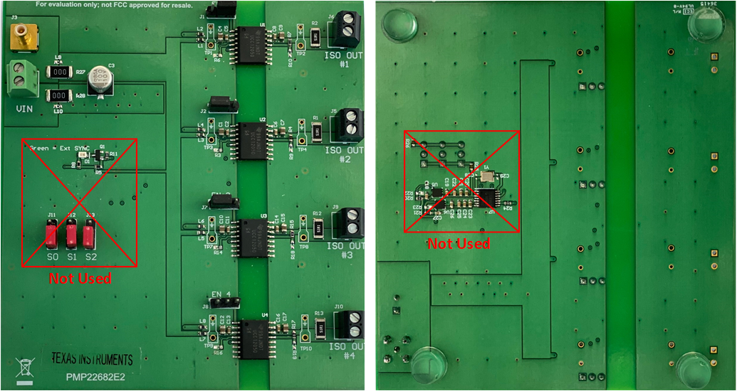
This reference design uses four, UCC12050 High-Efficiency, Low-EMI, 5-kVRMS Reinforced Isolation, DC-DC Converters on a single printed circuit board. The reference design includes additional provisions such as ferrite beads for optimized low-EMI emissions. Output voltages, VISO, can be selected for 3.3 V, 3.7 V, 5 V (default) and 5.4 V. Each of the four outputs includes a 100-mA, 500-mW load resistor commanding maximum output power by default but can easily be changed to accommodate any desired output load, up to 500 mW for any single converter. A single SMB input connector (J3) is included to allow easy and convenient connection to the input voltage source through a shielded input cable. The primary intent of this reference design is to investigate the impact that multiple high frequency converters have on EMI according to the CISPR 32, class B test standard. Applications include isolated bias supplies for isolated data converters, amplifiers and motor drivers used in industrial, factory automation and grid infrastructure systems.
 Figure 1-1 Top and Bottom Board View