SNOSB80C February 2011 – October 2015 LMP8350
PRODUCTION DATA.
1 Features
- Differential Input and Output
- Tri-Level Power Settings with Shutdown
- Ultra Low HD2/HD3 and THD+N Distortion
- Adjustable Output Common-Mode Level
- Fully-Balanced Differential Architecture
- Single- or Dual-Supply Operation
- Operating Voltage Range 4.5 V to 12 V
- Supply Current 3 mA to 13 mA
- Total THD+N at 1 KHz 0.000097%
- HD2 / HD3 Distortion at 1 KHz < –124 dBc
- Bandwidth 118 mHz
- Settling to 0.1% 20 ns
- Low Offset Drift 0.4 µV/°C
- Offset Voltage 80 µV
- Voltage Noise 4.6 nV/Hz
- Operating Temperature Range −40°C to +85°C
2 Applications
- High-Resolution Differential ADC Drivers
- Portable Instrumentation
- Precision Line Drivers
3 Description
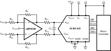
The LMP8350 device is an ultra low distortion fully-differential amplifier designed for driving high-performance precision analog-to-digital converters (ADC). As part of the PowerWise™ family, a unique mode enable pin allows the user to choose from three different operating modes, trading power consumption for dynamic performance.
The high power mode is optimized for highest AC performance. The low noise, wide bandwidth, and fast slew rate make the LMP8350 ideal for driving 24-bit ADCs with input sampling rates of 10 MHz or less. The medium power mode is optimized for precision DC performance, and can be used to drive 24-bit ADCs with input sampling rates of 6 MHz or less. The low power mode is a trade-off between AC performance and quiescent current for power-sensitive applications. The disable mode fully shuts down the amplifier for further standby power savings.
The fully differential architecture of this device allows for easy implementation of a single-ended to fully-differential output conversion. Driving a 3-Vpp, 1-kHz output sine wave with the amplifier powered by ±3.3-V rails in high power mode yields 0.000098% THD+N.
The LMP8350 is part of the LMP™ precision amplifier family, and is offered in the 8-pin SOIC package, with an operating temperature range of −40°C to +85°C.
Device Information(1)
| PART NUMBER | PACKAGE | BODY SIZE (NOM) |
|---|---|---|
| LMP8350 | SOIC (8) | 3.91 mm × 4.90 mm |
- For all available packages, see the orderable addendum at the end of the data sheet.
Typical Application
