SLRS021D December 1967 – January 2017 SN55451B , SN55452B , SN55453B , SN55454B , SN75451B , SN75452B , SN75453B , SN75454B
PRODUCTION DATA.
- 1 Features
- 2 Applications
- 3 Description
- 4 Revision History
- 5 Device Comparison Table
- 6 Pin Configuration and Functions
- 7 Specifications
- 8 Parameter Measurement Information
- 9 Detailed Description
- 10Application and Implementation
- 11Power Supply Recommendations
- 12Layout
- 13Device and Documentation Support
- 14Mechanical, Packaging, and Orderable Information
パッケージ・オプション
デバイスごとのパッケージ図は、PDF版データシートをご参照ください。
メカニカル・データ(パッケージ|ピン)
- D|8
- P|8
- PS|8
サーマルパッド・メカニカル・データ
- PS|8
発注情報
1 Features
2 Applications
- High-Speed Logic Buffers
- Power Drivers
- Lamp Drivers
- LED Drivers
- Line Drivers
- Memory Drivers
3 Description
The SN5545xB and SN7545xB devices are dual-peripheral drivers designed for use in systems that employ TTL logic. This family is functionally interchangeable with and replaces the SN75450 family and the SN75450A family devices manufactured previously. The speed of the devices is equal to that of the SN75450 family, and the parts are designed to ensure freedom from latch-up. Diode-clamped inputs simplify circuit design.
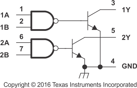
The SNx5451B, SNx5452B, SNx5453B, and SNx5454B devices are dual peripheral AND, NAND, OR, and NOR drivers, respectively (assuming positive logic), with the output of the logic gates internally connected to the bases of the npn output transistors.
The SN5545xB drivers are characterized for operation over the full military range of –55°C to 125°C. The SN7545xB drivers are characterized for operation from 0°C to 70°C.
Device Information(1)
| PART NUMBER | PACKAGE | BODY SIZE (NOM) |
|---|---|---|
| SN7545xBP | PDIP (8) | 9.81 mm × 6.35 mm |
| SN7545xBD | SOIC (8) | 4.90 mm × 3.90 mm |
| SN7545xBPS | SO (8) | 6.20 mm x 5.30 mm |
| SN5545xBJG | CDIP (8) | 9.60 mm × 6.67 mm |
| SN5545xBFK | LCCC (20) | 8.89 mm × 8.89 mm |
- For all available packages, see the orderable addendum at the end of the data sheet.
