JAJSFW1E June 2017 – March 2019 66AK2G12
PRODUCTION DATA.
- 1デバイスの概要
- 2改訂履歴
- 3Device Comparison
-
4Terminal Configuration and Functions
- 4.1 Pin Diagram
- 4.2 Pin Attributes
- 4.3 Signal Descriptions
- 4.4 Pin Multiplexing
- 4.5 Connections for Unused Pins
-
5Specifications
- 5.1 Absolute Maximum Ratings
- 5.2 ESD Ratings
- 5.3 Power-On-Hour (POH) Limits
- 5.4 Recommended Operating Conditions
- 5.5 Operating Performance Points
- 5.6 Power Consumption Summary
- 5.7
Electrical Characteristics
- Table 5-2 DDR3L SSTL DC Electrical Characteristics
- Table 5-3 I2C OPEN DRAIN DC Electrical Characteristics
- Table 5-4 Oscillators DC Electrical Characteristics
- Table 5-5 LVDS Input Buffer DC Electrical Characteristics
- Table 5-6 LVDS Output Buffer DC Electrical Characteristics
- Table 5-7 MLB LVDS Buffers DC Electrical Characteristics
- Table 5-8 PORn DC Electrical Characteristics
- Table 5-9 1.8-Volt I/O LVCMOS DC Electrical Characteristics
- Table 5-10 3.3-Volt I/O LVCMOS DC Electrical Characteristics
- 5.7.1 USB0_PHY and USB1_PHY DC Electrical Characteristics
- 5.7.2 PCIe SERDES DC Electrical Characteristics
- 5.8 Thermal Resistance Characteristics for ABY Package
- 5.9
Timing and Switching Characteristics
- 5.9.1 Power Supply Sequencing
- 5.9.2 Reset Timing
- 5.9.3
Clock Specifications
- 5.9.3.1 Input Clocks / Oscillators
- 5.9.3.2 Optional LVDS Clock Inputs Not Used
- 5.9.3.3 Optional Audio Oscillator (AUDOSC) with External Crystal Circuit
- 5.9.3.4 Optional Audio Oscillator (AUDOSC) with External LVCMOS Clock Source
- 5.9.3.5 Optional Audio Oscillator (AUDOSC) Not Used
- 5.9.3.6 Optional USB PHY Reference Clock
- 5.9.3.7 PCIe Reference Clock
- 5.9.3.8 Output Clocks
- 5.9.3.9 PLLs
- 5.9.3.10 Recommended Clock and Control Signal Transition Behavior
- 5.9.4
Peripherals
- 5.9.4.1 DCAN
- 5.9.4.2 DSS
- 5.9.4.3 DDR EMIF
- 5.9.4.4
EMAC
- 5.9.4.4.1 EMAC MDIO Interface Timings
- 5.9.4.4.2
EMAC MII Timings
- Table 5-28 Timing Requirements for MII_RXCLK—MII Operation
- Table 5-29 Timing Requirements for MII_TXCLK—MII Operation
- Table 5-30 Timing Requirements for EMAC MII Receive 10 Mbps and 100 Mbps
- Table 5-31 Switching Characteristics Over Recommended Operating Conditions for EMAC MII Transmit 10 Mbps and 100 Mbps
- 5.9.4.4.3
EMAC RMII Timings
- Table 5-32 Timing Requirements for EMAC RMII_REFCLK—RMII Operation
- Table 5-33 Timing Requirements for EMAC RMII Receive
- Table 5-34 Switching Characteristics Over Recommended Operating Conditions for EMAC RMII_REFCLK —RMII Operation
- Table 5-35 Switching Characteristics Over Recommended Operating Conditions for EMAC RMII Transmit 10 Mbps and 100 Mbps
- 5.9.4.4.4
EMAC RGMII Timings
- Table 5-36 Timing Requirements for RGMII_RXC—RGMII Operation
- Table 5-37 Timing Requirements for EMAC RGMII Input Receive for 10 Mbps, 100 Mbps, and 1000 Mbps
- Table 5-38 Switching Characteristics Over Recommended Operating Conditions for Transmit - RGMII operation for 10 Mbps, 100 Mbps, and 1000 Mbps
- Table 5-39 Switching Characteristics Over Recommended Operating Conditions for EMAC RGMII Transmit - RGMII_TXD[3:0], and RGMII_TXCTL - RGMII Mode
- Table 5-40 Switching Characteristics Over Recommended Operating Conditions for EMAC RGMII Transmit - RGMII_TXD[3:0], and RGMII_TXCTL - RGMII ID Mode
- 5.9.4.5 GPMC
- 5.9.4.6 I2C
- 5.9.4.7 McASP
- 5.9.4.8 McBSP
- 5.9.4.9 MLB
- 5.9.4.10
MMC/SD
- Table 5-60 MMC Timing Conditions
- Table 5-61 Timing Requirements for MMC0_CMD and MMC0_DATn
- Table 5-62 Timing Requirements for MMC1_CMD and MMC1_DATn when operating in SDR mode
- Table 5-63 Timing Requirements for MMC1_CMD and MMC1_DATn when operating in DDR mode
- Table 5-64 Switching Characteristics for MMCi_CLK
- Table 5-65 Switching Characteristics for MMC0_CMD and MMC0_DATn—HSPE=0
- Table 5-66 Switching Characteristics for MMC1_CMD and MMC1_DATn—HSPE=0 when operating in SDR mode
- Table 5-67 Switching Characteristics for MMC1_CMD and MMC1_DATn—HSPE=0 when operating in DDR mode
- 5.9.4.11 PCIESS
- 5.9.4.12
PRU-ICSS
- 5.9.4.12.1 Programmable Real-Time Unit (PRU-ICSS PRU)
- 5.9.4.12.2 PRU-ICSS EtherCAT (PRU-ICSS ECAT)
- 5.9.4.12.3 PRU-ICSS MII_RT and Switch
- 5.9.4.12.4 PRU-ICSS Universal Asynchronous Receiver Transmitter (PRU-ICSS UART)
- 5.9.4.12.5 PRU-ICSS PRU Sigma Delta and EnDAT Modes
- 5.9.4.13 QSPI
- 5.9.4.14 SPI
- 5.9.4.15 Timers
- 5.9.4.16 UART
- 5.9.4.17 USB
- 5.9.5 Emulation and Debug Subsystem
- 6Detailed Description
-
7Applications, Implementation, and Layout
- 7.1
DDR3L Board Design and Layout Guidelines
- 7.1.1 DDR3L General Board Layout Guidelines
- 7.1.2
DDR3L Board Design and Layout Guidelines
- 7.1.2.1 Board Designs
- 7.1.2.2 DDR3L Device Combinations
- 7.1.2.3 DDR3L Interface Schematic
- 7.1.2.4 Compatible JEDEC DDR3L Devices
- 7.1.2.5 PCB Stackup
- 7.1.2.6 Placement
- 7.1.2.7 DDR3L Keepout Region
- 7.1.2.8 Bulk Bypass Capacitors
- 7.1.2.9 High-Speed Bypass Capacitors
- 7.1.2.10 Net Classes
- 7.1.2.11 DDR3L Signal Termination
- 7.1.2.12 VREF_DDR Routing
- 7.1.2.13 VTT
- 7.1.2.14 CK and ADDR_CTRL Topologies and Routing Definition
- 7.1.2.15 Data Topologies and Routing Definition
- 7.1.2.16 Routing Specification
- 7.2 High Speed Differential Signal Routing Guidance
- 7.3 Power Distribution Network (PDN) Implementation Guidance
- 7.4 Single-Ended Interfaces
- 7.5 Clock Routing Guidelines
- 7.1
DDR3L Board Design and Layout Guidelines
- 8Device and Documentation Support
- 9Mechanical Packaging and Orderable Information
パッケージ・オプション
デバイスごとのパッケージ図は、PDF版データシートをご参照ください。
メカニカル・データ(パッケージ|ピン)
- ABY|625
サーマルパッド・メカニカル・データ
発注情報
7.1.2.16.1 CK and ADDR_CTRL Routing Specification
Skew within the CK and ADDR_CTRL net classes directly reduces setup and hold margin and, thus, this skew must be controlled. The only way to practically match lengths on a PCB is to lengthen the shorter traces up to the length of the longest net in the net class and its associated clock. A metric to establish this maximum length is Manhattan distance. The Manhattan distance between two points on a PCB is the length between the points when connecting them only with horizontal or vertical segments. A reasonable trace route length is to within a percentage of its Manhattan distance. CACLM is defined as Clock Address Control Longest Manhattan distance.
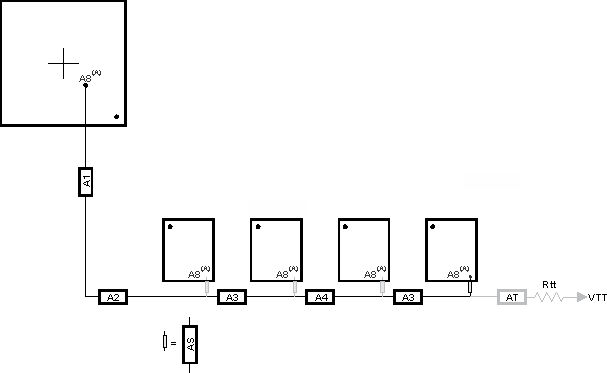
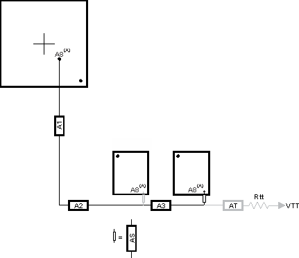
Given the clock and address pin locations on the processor and the DDR3L memories, the maximum possible Manhattan distance can be determined given the placement. Figure 7-20 and Figure 7-21 show this distance for four loads and two loads, respectively. It is from this distance that the specifications on the lengths of the transmission lines for the address bus are determined. CACLM is determined similarly for other address bus configurations; that is, it is based on the longest net of the CK/ADDR_CTRL net class. For CK and ADDR_CTRL routing, these specifications are contained in Table 7-11.
 Figure 7-20 Four Address Loads on One Side of PCB
  Figure 7-21 Two Address Loads on One Side of PCB
 Table 7-11 CK and ADDR_CTRL Routing Specification(2)(3)
| NO. | PARAMETER | MIN | TYP | MAX | UNIT |
|---|---|---|---|---|---|
| CARS31 | A1+A2 length | 500(1) | ps | ||
| CARS32 | A1+A2 skew | 29 | ps | ||
| CARS33 | A3 length | 125 | ps | ||
| CARS34 | A3 skew(4) | 6 | ps | ||
| CARS35 | A3 skew(5) | 6 | ps | ||
| CARS36 | A4 length | 125 | ps | ||
| CARS37 | A4 skew | 6 | ps | ||
| CARS38 | AS length | 5(1) | 17 | ps | |
| CARS39 | AS skew | 1.3(1) | 14 | ps | |
| CARS310 | AS+/AS- length | 5 | 12 | ps | |
| CARS311 | AS+/AS- skew | 1 | ps | ||
| CARS312 | AT length(6) | 75 | ps | ||
| CARS313 | AT skew(7) | 14 | ps | ||
| CARS314 | AT skew(8) | 1 | ps | ||
| CARS315 | CK/ADDR_CTRL trace length | 1020 | ps | ||
| CARS316 | Vias per trace | 3(1) | vias | ||
| CARS317 | Via count difference | 1(15) | vias | ||
| CARS318 | Center-to-center CK to other DDR3L trace spacing(9) | 4w | |||
| CARS319 | Center-to-center ADDR_CTRL to other DDR3L trace spacing(9)(10) | 4w | |||
| CARS320 | Center-to-center ADDR_CTRL to other ADDR_CTRL trace spacing(9) | 3w | |||
| CARS321 | CK center-to-center spacing(11)(12) | ||||
| CARS322 | CK spacing to other net(9) | 4w | |||
| CARS323 | Rcp(13) | Zo-1 | Zo | Zo+1 | Ω |
| CARS324 | Rtt(13)(14) | Zo-5 | Zo | Zo+5 | Ω |
- Max value is based upon conservative signal integrity approach. This value could be extended only if detailed signal integrity analysis of rise time and fall time confirms desired operation.
- The use of vias should be minimized.
- Additional bypass capacitors are required when using the DVDD_DDR plane as the reference plane to allow the return current to jump between the DVDD_DDR plane and the ground plane when the net class switches layers at a via.
- Non-mirrored configuration (all DDR3L memories on same side of PCB).
- Mirrored configuration (one DDR3L device on top of the board and one DDR3L device on the bottom).
- While this length can be increased for convenience, its length should be minimized.
- ADDR_CTRL net class only (not CK net class). Minimizing this skew is recommended, but not required.
- CK net class only.
- Center-to-center spacing is allowed to fall to minimum 2w for up to 1250 mils of routed length.
- The ADDR_CTRL net class of the other DDR EMIF is considered other DDR3L trace spacing.
- CK spacing set to ensure proper differential impedance.
- The most important thing to do is control the impedance so inadvertent impedance mismatches are not created. Generally speaking, center-to-center spacing should be either 2w or slightly larger than 2w to achieve a differential impedance equal to twice the singleended impedance, Zo.
- Source termination (series resistor at driver) is specifically not allowed.
- Termination values should be uniform across the net class.
- Via count difference may increase by 1 only if accurate 3D modeling of the signal flight times – including accurately modeled signal propagation through vias – has been applied to ensure all segment skew maximums are not exceeded.