SPRS866G November 2012 – October 2017 66AK2H06 , 66AK2H12 , 66AK2H14
PRODUCTION DATA.
- 1 Device Overview
- 2 Revision History
- 3 Device Comparison
- 4 Terminal Configuration and Functions
- 5 Specifications
- 6 C66x CorePac
- 7 ARM CorePac
- 8 Memory, Interrupts, and EDMA for 66AK2Hxx
- 9 System Interconnect
-
10Device Boot and Configuration
- 10.1
Device Boot
- 10.1.1 Boot Sequence
- 10.1.2
Boot Modes Supported
- 10.1.2.1 Boot Device Field
- 10.1.2.2 Device Configuration Field
- 10.1.2.3 Serial Rapid I/O Boot Device Configuration
- 10.1.2.4 Ethernet (SGMII) Boot Device Configuration
- 10.1.2.5
Boot Parameter Table
- 10.1.2.5.1 EMIF16 Boot Parameter Table
- 10.1.2.5.2 SRIO Boot Parameter Table
- 10.1.2.5.3 Ethernet Boot Parameter Table
- 10.1.2.5.4 PCIe Boot Parameter Table
- 10.1.2.5.5 I2C Boot Parameter Table
- 10.1.2.5.6 SPI Boot Parameter Table
- 10.1.2.5.7 HyperLink Boot Parameter Table
- 10.1.2.5.8 UART Boot Parameter Table
- 10.1.2.5.9 NAND Boot Parameter Table
- 10.1.2.5.10 DDR3 Configuration Table
- 10.1.2.6 Second-Level Bootloaders
- 10.1.3 SoC Security
- 10.1.4 System PLL Settings
- 10.2
Device Configuration
- 10.2.1 Device Configuration at Device Reset
- 10.2.2 Peripheral Selection After Device Reset
- 10.2.3
Device State Control Registers
- 10.2.3.1 Device Status (DEVSTAT) Register
- 10.2.3.2 Device Configuration Register
- 10.2.3.3 JTAG ID (JTAGID) Register Description
- 10.2.3.4 Kicker Mechanism (KICK0 and KICK1) Register
- 10.2.3.5 DSP Boot Address Register (DSP_BOOT_ADDRn)
- 10.2.3.6 LRESETNMI PIN Status (LRSTNMIPINSTAT) Register
- 10.2.3.7 LRESETNMI PIN Status Clear (LRSTNMIPINSTAT_CLR) Register
- 10.2.3.8 Reset Status (RESET_STAT) Register
- 10.2.3.9 Reset Status Clear (RESET_STAT_CLR) Register
- 10.2.3.10 Boot Complete (BOOTCOMPLETE) Register
- 10.2.3.11 Power State Control (PWRSTATECTL) Register
- 10.2.3.12 NMI Event Generation to C66x CorePac (NMIGRx) Register
- 10.2.3.13 IPC Generation (IPCGRx) Registers
- 10.2.3.14 IPC Acknowledgment (IPCARx) Registers
- 10.2.3.15 IPC Generation Host (IPCGRH) Register
- 10.2.3.16 IPC Acknowledgment Host (IPCARH) Register
- 10.2.3.17 Timer Input Selection Register (TINPSEL)
- 10.2.3.18 Timer Output Selection Register (TOUTPSEL)
- 10.2.3.19 Reset Mux (RSTMUXx) Register
- 10.2.3.20 Device Speed (DEVSPEED) Register
- 10.2.3.21 ARM Endian Configuration Register 0 (ARMENDIAN_CFGr_0), r=0..7
- 10.2.3.22 ARM Endian Configuration Register 1 (ARMENDIAN_CFGr_1), r=0..7
- 10.2.3.23 ARM Endian Configuration Register 2 (ARMENDIAN_CFGr_2), r=0..7
- 10.2.3.24 Chip Miscellaneous Control (CHIP_MISC_CTL0) Register
- 10.2.3.25 Chip Miscellaneous Control (CHIP_MISC_CTL1) Register
- 10.2.3.26 System Endian Status Register (SYSENDSTAT)
- 10.2.3.27 SYNECLK_PINCTL Register
- 10.2.3.28 USB PHY Control (USB_PHY_CTLx) Registers
- 10.1
Device Boot
-
1166AK2Hxx Peripheral Information
- 11.1 Recommended Clock and Control Signal Transition Behavior
- 11.2 Power Supplies
- 11.3 Power Sleep Controller (PSC)
- 11.4 Reset Controller
- 11.5
Main PLL, ARM PLL, DDR3A PLL, DDR3B PLL, PASS PLL and the PLL Controllers
- 11.5.1 Main PLL Controller Device-Specific Information
- 11.5.2
PLL Controller Memory Map
- 11.5.2.1 PLL Secondary Control Register (SECCTL)
- 11.5.2.2 PLL Controller Divider Register (PLLDIV3 and PLLDIV4)
- 11.5.2.3 PLL Controller Clock Align Control Register (ALNCTL)
- 11.5.2.4 PLLDIV Divider Ratio Change Status Register (DCHANGE)
- 11.5.2.5 SYSCLK Status Register (SYSTAT)
- 11.5.2.6 Reset Type Status Register (RSTYPE)
- 11.5.2.7 Reset Control Register (RSTCTRL)
- 11.5.2.8 Reset Configuration Register (RSTCFG)
- 11.5.2.9 Reset Isolation Register (RSISO)
- 11.5.3 Main PLL Control Registers
- 11.5.4 ARM PLL Control Registers
- 11.5.5 Main PLL Controller, ARM, SRIO, HyperLink, PCIe, USB Clock Input Electrical Data and Timing
- 11.6 DDR3A PLL and DDR3B PLL
- 11.7 PASS PLL
- 11.8 External Interrupts
- 11.9 DDR3A and DDR3B Memory Controllers
- 11.10 I2C Peripheral
- 11.11 SPI Peripheral
- 11.12 HyperLink Peripheral
- 11.13 UART Peripheral
- 11.14 PCIe Peripheral
- 11.15 Packet Accelerator
- 11.16 Security Accelerator
- 11.17 Network Coprocessor Gigabit Ethernet (GbE) Switch Subsystem
- 11.18 SGMII and XFI Management Data Input/Output (MDIO)
- 11.19 Ten-Gigabit Ethernet (10GbE) Switch Subsystem
- 11.20 Timers
- 11.21 Serial RapidIO (SRIO) Port
- 11.22 General-Purpose Input/Output (GPIO)
- 11.23 Semaphore2
- 11.24 Universal Serial Bus 3.0 (USB 3.0)
- 11.25 EMIF16 Peripheral
- 11.26 Emulation Features and Capability
- 11.27 Debug Port (EMUx)
- 12Device and Documentation Support
- 13Mechanical, Packaging, and Orderable Information
パッケージ・オプション
デバイスごとのパッケージ図は、PDF版データシートをご参照ください。
メカニカル・データ(パッケージ|ピン)
- AAW|1517
サーマルパッド・メカニカル・データ
発注情報
7 ARM CorePac
The ARM CorePac is added in the 66AK2Hxx to enable the ability for layer 2 and layer 3 processing on-chip. Operations such as traffic control, local O&M, NBAP/FP termination, and SCTP processing can all be performed with the Cortex-A15 processor core.
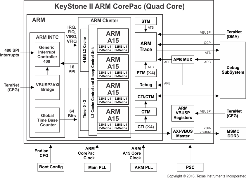
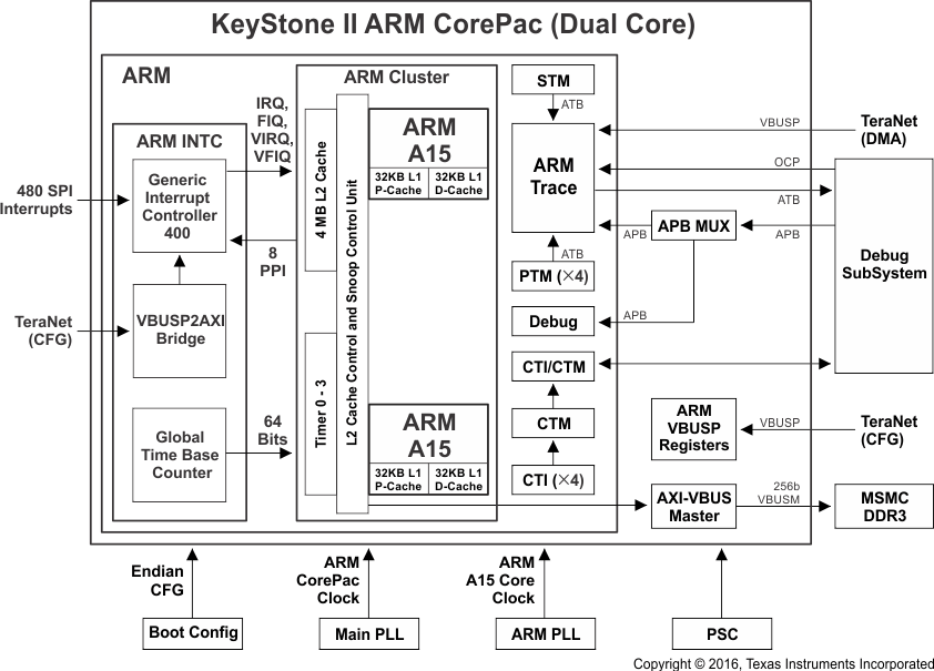
The ARM CorePac of the 66AK2Hxx integrates one or more Cortex-A15 processor clusters with additional logic for bus protocol conversion, emulation, interrupt handling, and debug related enhancements. The Cortex-A15 processor is an ARMv7A-compatible, multi-issue out-of-order superscalar execution engine with integrated L1 caches. The implementation also supports advanced SIMDv2 (NEON technology) and VFPv4 (vector floating point) architecture extensions, security, virtualization, LPAE (large physical address extension), and multiprocessing extensions. The ARM CorePac includes a 4MB L2 cache and support for AMBA4 AXI and AXI coherence extension (ACE) protocols. An interrupt controller is included in the ARM CorePac to handle host interrupt requests in the system. For more information, see the KeyStone II Architecture ARM CorePac User's Guide.
The ARM CorePac has three functional clock domains, including a high-frequency clock domain used by the Cortex-A15. The high-frequency domain is isolated from the rest of the device by asynchronous bridges.
Figure 7-1 and Figure 7-2 show the ARM CorePac.
 Figure 7-1 66AK2H12 ARM CorePac Block Diagram
 Figure 7-2 66AK2H06 ARM CorePac Block Diagram
7.1 Features
The key features of the Quad Core ARM CorePac are as follows:
- One or more Cortex-A15 processors, each containing:
- Cortex-A15 processor revision R2P4.
- ARM architecture version 7 ISA.
- Multi-issue, out-of-order, superscalar pipeline.
- L1 and L2 instruction and data cache of 32KB, 2-way, 16 word line with 128-bit interface.
- Integrated L2 cache of 4MB, 16-way, 16-word line, 128-bit interface to L1 along with ECC/parity.
- Includes the NEON™ media coprocessor (NEON), which implements the advanced SIMDv2 media processing architecture and the VFPv4 Vector Floating Point architecture.
- The external interface uses the AXI protocol configured to 128-bit data width.
- Includes the System Trace Macrocell (STM) support for noninvasive debugging.
- Implements the ARMv7 debug with watchpoint and breakpoint registers and 32-bit advanced peripheral bus (APB) slave interface to CoreSight™ debug systems.
- Interrupt controller
- Supports up to 480 interrupt requests
- Emulation/debug
- Compatible with CoreSight architecture
7.2 System Integration
The ARM CorePac integrates the following group of submodules.
- Cortex-A15 Processors: Provides a high processing capability, including the NEON technology for mobile multimedia acceleration. The Cortex-A15 communicates with the rest of the ARM CorePac through an AXI bus with an AXI2VBUSM bridge and receives interrupts from the ARM CorePac interrupt controller (ARM INTC).
- Interrupt Controller: Handles interrupts from modules outside of the ARM CorePac (for details, see Section 7.3.3).
- Clock Divider: Provides the required divided clocks to the internal modules of the ARM CorePac and has a clock input from the ARM PLL and the Main PLL
- In-Circuit Emulator: Fully compatible with CoreSight architecture and enables debugging capabilities.
7.3 ARM Cortex-A15 Processor
7.3.1 Overview
The ARM Cortex-A15 processor incorporates the technologies available in the ARM7™ architecture. These technologies include NEON for media and signal processing and Jazelle® RCT for acceleration of real-time compilers, Thumb®-2 technology for code density, and the VFPv4 floating point architecture. For details, see the ARM Cortex-A15 Processor Technical Reference Manual.
7.3.2 Features
Table 7-1 shows the features supported by the Cortex-A15 processor core.
Table 7-1 Cortex-A15 Processor Core Supported Features
| FEATURES | DESCRIPTION |
|---|---|
| ARM version 7-A ISA | Standard Cortex-A15 processor instruction set + Thumb2, ThumbEE, JazelleX Java accelerator, and media extensions |
| Backward compatible with previous ARM ISA versions | |
| Cortex-A15 processor version | R2P4 |
| Integer core | Main core for processing integer instructions |
| NEON core | Gives greatly enhanced throughput for media workloads and VFP-Lite support |
| Architecture Extensions | Security, virtualization and LPAE (40-bit physical address) extensions |
| L1 Lcache and Dcache | 32KB, 2-way, 16 word line, 128 bit interface |
| L2 cache | 4096KB, 16-way, 16 word line, 128 bit interface to L1, ECC/Parity is supported shared between cores |
| L2 valid bits cleared by software loop or by hardware | |
| Cache Coherency | Support for coherent memory accesses between A15 cores and other noncore master peripherals (Ex: EDMA) in the DDR3A and MSMC SRAM space. |
| Branch target address cache | Dynamic branch prediction with Branch Target Buffer (BTB) and Global History Buffer (GHB), a return stack, and an indirect predictor |
| Enhanced memory management unit | Mapping sizes are 4KB, 64KB, 1MB, and 16MB |
| Buses | 128b AXI4 internal bus from Cortex-A15 converted to a 256b VBUSM to interface (through the MSMC) with MSMC SRAM, DDR EMIF, ROM, Interrupt controller and other system peripherals |
| Noninvasive Debug Support | Processor instruction trace using 4x Program Trace Macrocell (CoreSight PTM), Data trace (print-f style debug) using System Trace Macrocell (CoreSight STM) and Performance Monitoring Units (PMU) |
| Misc Debug Support | JTAG based debug and Cross triggering |
| Clocking | Dedicated ARM PLL for flexible clocking scenarios |
| Voltage | SmartReflex voltage domain for automatic voltage scaling |
| Power | Support for standby modes and separate core power domains for additional leakage power reduction |
7.3.3 ARM Interrupt Controller
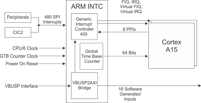
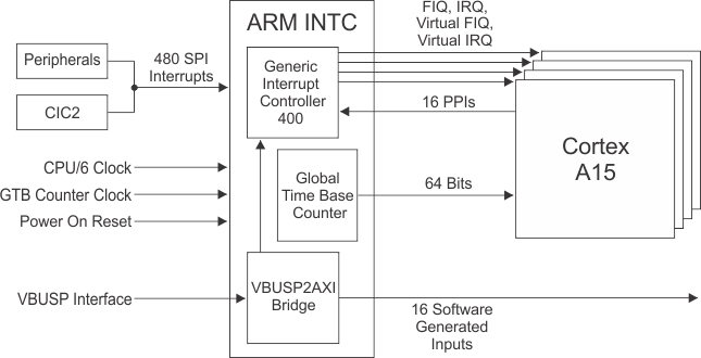
The ARM CorePac interrupt controller (AINTC) is responsible for prioritizing all service requests from the system peripherals and the secondary interrupt controller CIC2 and then generating either nIRQ or nFIQ to the Cortex-A15 processor. The type of the interrupt (nIRQ or nFIQ) and the priority of the interrupt inputs are programmable. The AINTC interfaces to the Cortex-A15 processor via the AXI port through an VBUS2AXI bridge and runs at half the processor speed. It has the capability to handle up to 480 requests, which can be steered/prioritized as A15 nFIQ or nIRQ interrupt requests.
The general features of the AINTC are:
- Up to 480 level sensitive shared peripheral interrupts (SPI) inputs
- Individual priority for each interrupt input
- Each interrupt can be steered to nFIQ or nIRQ
- Independent priority sorting for nFIQ and nIRQ
- Secure mask flag
On the chip level, there is a dedicated chip level interrupt controller to serve the ARM interrupt controller. See Section 8.3 for more details.
Figure 7-3 and Figure 7-4 show an overall view of the ARM CorePac Interrupt Controller.
 Figure 7-3 ARM Interrupt Controller for Two Cortex-A15 Processor Cores
 Figure 7-4 ARM Interrupt Controller for Four Cortex-A15 Processor Cores
7.3.4 Endianess
The ARM CorePac can operate in either little-endian or big-endian mode. When the ARM CorePac is in little-endian mode and the rest of the system is in big-endian mode, the bridges in the ARM CorePac are responsible for performing the endian conversion.
7.4 CFG Connection
The ARM CorePac has two slave ports. The 66AK2Hxx masters cannot access the ARM CorePac internal memory space.
- Slave port 0 (TeraNet 3P_A) is a 32-bit-wide port used for the ARM Trace module.
- Slave port 1 (TeraNet 3P_B) is a 32-bit-wide port used to access the rest of the system configuration.
7.5 Main TeraNet Connection
One master port comes out of the ARM CorePac. The master port is a 256-bit-wide port for the transactions going to the MSMC and DDR_EMIF data spaces.
7.6 Clocking and Reset
7.6.1 Clocking
The ARM CorePac includes a dedicated embedded DPLL (ARM PLL). The Cortex-A15 processor core clocks are sourced from this ARM PLL Controller. The Cortex-A15 processor core clock has a maximum frequency of 1.4 GHz. The ARM CorePac subsytem also uses the SYSCLK1 clock source from the main PLL which is locally divided (/1, /3 and /6) and provided to certain submodules inside the ARM CorePac. AINTC sub module runs at a frequency of SYSCLK1/6.
7.6.2 Reset
The ARM CorePac does not support local reset. It is reset whenever the device is under reset. In addition, the interrupt controller (AINTC) can only be reset during POR and RESETFULL. AINTC also resets whenever device is under reset.
For the complete programming model, refer to the KeyStone II Architecture ARM CorePac User's Guide.