SNAS518J July 2011 – July 2015 ADC12D1800RF
PRODUCTION DATA.
- 1 Device Overview
- 2 Revision History
- 3 Pin Configuration and Functions
-
4 Specifications
- 4.1 Absolute Maximum Ratings
- 4.2 ESD Ratings
- 4.3 Recommended Operating Conditions
- 4.4 Thermal Information
- 4.5 Converter Electrical Characteristics: Static Converter Characteristics
- 4.6 Converter Electrical Characteristics: Dynamic Converter Characteristics
- 4.7 Converter Electrical Characteristics: Analog Input / Output and Reference Characteristics
- 4.8 Converter Electrical Characteristics: I-Channel to Q-Channel Characteristics
- 4.9 Converter Electrical Characteristics: Sampling Clock Characteristics
- 4.10 Converter Electrical Characteristics: AutoSync Feature Characteristics
- 4.11 Converter Electrical Characteristics: Digital Control and Output Pin Characteristics
- 4.12 Converter Electrical Characteristics: Power Supply Characteristics
- 4.13 Converter Electrical Characteristics: AC Electrical Characteristics
- 4.14 Converter Electrical Characteristics: Serial Port Interface
- 4.15 Converter Electrical Characteristics Calibration
- 4.16 Typical Characteristics
-
5 Detailed Description
- 5.1 Overview
- 5.2 Functional Block Diagram
- 5.3 Feature Description
- 5.4 Device Functional Modes
- 5.5
Programming
- 5.5.1
Control Modes
- 5.5.1.1
Non-Extended Control Mode
- 5.5.1.1.1 Dual Edge Sampling Pin (DES)
- 5.5.1.1.2 Non-Demultiplexed Mode Pin (NDM)
- 5.5.1.1.3 Dual Data Rate Phase Pin (DDRPh)
- 5.5.1.1.4 Calibration Pin (CAL)
- 5.5.1.1.5 Calibration Delay Pin (CalDly)
- 5.5.1.1.6 Power Down I-channel Pin (PDI)
- 5.5.1.1.7 Power Down Q-channel Pin (PDQ)
- 5.5.1.1.8 Test Pattern Mode Pin (TPM)
- 5.5.1.1.9 Full-Scale Input Range Pin (FSR)
- 5.5.1.1.10 AC / DC-Coupled Mode Pin (VCMO)
- 5.5.1.1.11 LVDS Output Common-mode Pin (VBG)
- 5.5.1.2 Extended Control Mode
- 5.5.1.1
Non-Extended Control Mode
- 5.5.1
Control Modes
- 5.6 Register Maps
- 6 Application and Implementation
- 7 Power Supply Recommendations
- 8 Layout
- 9 Device and Documentation Support
- 10Mechanical, Packaging, and Orderable Information
6 Application and Implementation
NOTE
Information in the following applications sections is not part of the TI component specification, and TI does not warrant its accuracy or completeness. TI’s customers are responsible for determining suitability of components for their purposes. Customers should validate and test their design implementation to confirm system functionality.
6.1 Application Information
6.1.1 Analog Inputs
The ADC12D1800RF will continuously convert any signal which is present at the analog inputs, as long as a CLK signal is also provided to the device. This section covers important aspects related to the analog inputs including: acquiring the input, driving the ADC in DES Mode, the reference voltage and FSR, out-of-range indication, AC/DC-coupled signals, and single-ended input signals.
6.1.1.1 Acquiring the Input
The Aperture Delay, tAD, is the amount of delay, measured from the sampling edge of the clock input, after which the signal present at the input pin is sampled inside the device. Data is acquired at the rising edge of CLK+ in Non-DES Mode and both the falling and rising edge of CLK+ in DES Mode. In Non-DES Mode, the I- and Q-channels always sample data on the rising edge of CLK+. In DES Mode, i.e. DESI, DESQ, DESIQ, and DESCLKIQ, the I-channel samples data on the rising edge of CLK+ and the Q-channel samples data on the falling edge of CLK+. The digital equivalent of that data is available at the digital outputs a constant number of sampling clock cycles later for the DI, DQ, DId and DQd output busses, a.k.a. the latency, depending on the demultiplex mode which is selected. In addition to the latency, there is a constant output delay, tOD, before the data is available at the outputs. See tOD in Figure 4-2 to Figure 4-5. See tLAT, tAD, and tOD in Section 4.13.
6.1.1.2 Driving the ADC in DES Mode
The ADC12D1800RF can be configured as either a 2-channel, 1.8 GSPS device (Non-DES Mode) or a 1-channel 3.6 GSPS device (DES Mode). When the device is configured in DES Mode, there is a choice for with which input to drive the single-channel ADC. These are the 3 options:
DES – externally driving the I-channel input only. This is the default selection when the ADC is configured in DES Mode. It may also be referred to as “DESI” for added clarity.
DESQ – externally driving the Q-channel input only.
DESIQ, DESCLKIQ – externally driving both the I- and Q-channel inputs. VinI+ and VinQ+ should be driven with the exact same signal. VinI- and VinQ- should be driven with the exact same signal, which is the differential complement to the one driving VinI+ and VinQ+.
The input impedance for each I- and Q-input is 100Ω differential (or 50Ω single-ended), so the trace to each VinI+, VinI-, VinQ+, and VinQ- should always be 50Ω single-ended. If a single I- or Q-input is being driven, then that input will present a 100Ω differential load. For example, if a 50Ω single-ended source is driving the ADC, then a 1:2 balun will transform the impedance to 100Ω differential. However, if the ADC is being driven in DESIQ Mode, then the 100Ω differential impedance from the I-input will appear in parallel with the Q-input for a composite load of 50Ω differential and a 1:1 balun would be appropriate. See Figure 6-1 for an example circuit driving the ADC in DESIQ Mode. A recommended part selection is using the Mini-Circuits TC1-1-13MA+ balun with Ccouple = 0.22µF.
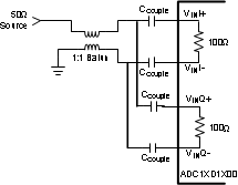 Figure 6-1 Driving DESIQ Mode
In the case that only one channel is used in Non-DES Mode or that the ADC is driven in DESI or DESQ Mode, the unused analog input should be terminated to reduce any noise coupling into the ADC. See Table 6-1 for details.
Table 6-1 Unused Analog Input Recommended Termination
| Mode | Power Down | Coupling | Recommended Termination |
|---|---|---|---|
| Non-DES | Yes | AC/DC | Tie Unused+ and Unused- to Vbg |
| DES/Non-DES | No | DC | Tie Unused+ and Unused- to Vbg |
| DES/Non-DES | No | AC | Tie Unused+ to Unused- |
6.1.1.3 FSR and the Reference Voltage
The full-scale analog differential input range (VIN_FSR) of the ADC12D1800RF is derived from an internal bandgap reference. In Non-ECM, this full-scale range must be set by the logic-high setting of the FSR Pin; see Section 5.5.1.1.9. The FSR Pin operates on both I- and Q-channels. In ECM, the full-scale range may be independently set for each channel via Addr:3h and Bh with 15 bits of precision; see Section 5.6.1. The best SNR is obtained with a higher full-scale input range, but better distortion and SFDR are obtained with a lower full-scale input range. It is not possible to use an external analog reference voltage to modify the full-scale range, and this adjustment should only be done digitally, as described.
A buffered version of the internal bandgap reference voltage is made available at the VBG Pin for the user. The VBG pin can drive a load of up to 80 pF and source or sink up to 100 μA. It should be buffered if more current than this is required. This pin remains as a constant reference voltage regardless of what full-scale range is selected and may be used for a system reference. VBG is a dual-purpose pin and it may also be used to select a higher LVDS output common-mode voltage; see Section 5.5.1.1.11.
6.1.1.4 Out-of-Range Indication
Differential input signals are digitized to 12 bits, based on the full-scale range. Signal excursions beyond the full-scale range, i.e. greater than +VIN_FSR/2 or less than -VIN_FSR/2, will be clipped at the output. An input signal which is above the FSR will result in all 1's at the output and an input signal which is below the FSR will result in all 0's at the output. When the conversion result is clipped for the I-channel input, the Out-of-Range I-channel (ORI) output is activated such that ORI+ goes high and ORI- goes low while the signal is out of range. This output is active as long as accurate data on either or both of the buses would be outside the range of 000h to FFFh. The Q-channel has a separate ORQ which functions similarly.
6.1.1.5 Maximum Input Range
The recommended operating and absolute maximum input range may be found in Section 4.3 and Section 4.1, respectively. Under the stated allowed operating conditions, each Vin+ and Vin- input pin may be operated in the range from 0V to 2.15V if the input is a continuous 100% duty cycle signal and from 0V to 2.5V if the input is a 10% duty cycle signal. The absolute maximum input range for Vin+ and Vin- is from -0.15V to 2.5V. These limits apply only for input signals for which the input common mode voltage is properly maintained.
6.1.1.6 AC-Coupled Input Signals
The ADC12D1800RF analog inputs require a precise common-mode voltage. This voltage is generated on-chip when AC-coupling Mode is selected. See Section 5.5.1.1.10 for more information about how to select AC-coupled Mode.
In AC-coupled Mode, the analog inputs must of course be AC-coupled. For an ADC12D1800RF used in a typical application, this may be accomplished by on-board capacitors, as shown in Figure 6-2. For the ADC12D1800RFRB, the SMA inputs on the Reference Board are directly connected to the analog inputs on the ADC12D1800RF, so this may be accomplished by DC blocks (included with the hardware kit).
When the AC-coupled Mode is selected, an analog input channel that is not used (e.g. in DES Mode) should be connected to AC ground, e.g. through capacitors to ground . Do not connect an unused analog input directly to ground.
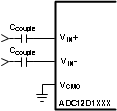 Figure 6-2 AC-coupled Differential Input
The analog inputs for the ADC12D1800RF are internally buffered, which simplifies the task of driving these inputs and the RC pole which is generally used at sampling ADC inputs is not required. If the user desires to place an amplifier circuit before the ADC, care should be taken to choose an amplifier with adequate noise and distortion performance, and adequate gain at the frequencies used for the application.
6.1.1.7 DC-Coupled Input Signals
In DC-coupled Mode, the ADC12D1800RF differential inputs must have the correct common-mode voltage. This voltage is provided by the device itself at the VCMO output pin. It is recommended to use this voltage because the VCMO output potential will change with temperature and the common-mode voltage of the driving device should track this change. Full-scale distortion performance falls off as the input common mode voltage deviates from VCMO. Therefore, it is recommended to keep the input common-mode voltage within 100 mV of VCMO (typical), although this range may be extended to ±150 mV (maximum). See VCMI in Section 4.7 and ENOB vs. VCMI in Section 4.16. Performance in AC- and DC-coupled Mode are similar, provided that the input common mode voltage at both analog inputs remains within 100 mV of VCMO.
6.1.1.8 Single-Ended Input Signals
The analog inputs of the ADC12D1800RF are not designed to accept single-ended signals. The best way to handle single-ended signals is to first convert them to differential signals before presenting them to the ADC. The easiest way to accomplish single-ended to differential signal conversion is with an appropriate balun-transformer, as shown in Figure 6-3.
 Figure 6-3 Single-Ended to Differential Conversion Using a Balun
When selecting a balun, it is important to understand the input architecture of the ADC. The impedance of the analog source should be matched to the ADC12D1800RF's on-chip 100Ω differential input termination resistor. The range of this termination resistor is specified as RIN in Section 4.7.
6.1.2 Clock Inputs
The ADC12D1800RF has a differential clock input, CLK+ and CLK-, which must be driven with an AC-coupled, differential clock signal. This provides the level shifting necessary to allow for the clock to be driven with LVDS, PECL, LVPECL, or CML levels. The clock inputs are internally terminated to 100Ω differential and self-biased. This section covers coupling, frequency range, level, duty-cycle, jitter, and layout considerations.
6.1.2.1 CLK Coupling
The clock inputs of the ADC12D1800RF must be capacitively coupled to the clock pins as indicated in Figure 6-4.
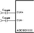 Figure 6-4 Differential Input Clock Connection
The choice of capacitor value will depend on the clock frequency, capacitor component characteristics and other system economic factors. For example, on the ADC12D1800RFRB, the capacitors have the value Ccouple = 4.7 nF which yields a high pass cutoff frequency, fc = 677.2 kHz.
6.1.2.2 CLK Frequency
Although the ADC12D1800RF is tested and its performance is ensured with a differential 1.8 GHz sampling clock, it will typically function well over the input clock frequency range; see fCLK(min) and fCLK(max) in Section 4.13. Operation up to fCLK(max) is possible if the maximum ambient temperatures indicated are not exceeded. Operating at sample rates above fCLK(max) for the maximum ambient temperature may result in reduced device reliability and product lifetime. This is due to the fact that higher sample rates results in higher power consumption and die temperatures. If fCLK < 300 MHz, enable LFS in the Control Register (Addr: 0h, Bit 8).
6.1.2.3 CLK Level
The input clock amplitude is specified as VIN_CLK in Section 4.9. Input clock amplitudes above the max VIN_CLK may result in increased input offset voltage. This would cause the converter to produce an output code other than the expected 2047/2048 when both input pins are at the same potential. Insufficient input clock levels will result in poor dynamic performance. Both of these results may be avoided by keeping the clock input amplitude within the specified limits of VIN_CLK.
6.1.2.4 CLK Duty Cycle
The duty cycle of the input clock signal can affect the performance of any A/D converter. The ADC12D1800RF features a duty cycle clock correction circuit which can maintain performance over the 20%-to-80% specified clock duty-cycle range. This feature is enabled by default and provides improved ADC clocking, especially in the Dual-Edge Sampling (DES) Mode.
6.1.2.5 CLK Jitter
High speed, high performance ADCs such as the ADC12D1800RF require a very stable input clock signal with minimum phase noise or jitter. ADC jitter requirements are defined by the ADC resolution (number of bits), maximum ADC input frequency and the input signal amplitude relative to the ADC input full scale range. The maximum jitter (the sum of the jitter from all sources) allowed to prevent a jitter-induced reduction in SNR is found to be
where tJ(MAX) is the rms total of all jitter sources in seconds, VIN(P-P) is the peak-to-peak analog input signal, VFSR is the full-scale range of the ADC, "N" is the ADC resolution in bits and fIN is the maximum input frequency, in Hertz, at the ADC analog input.
tJ(MAX) is the square root of the sum of the squares (RSS) sum of the jitter from all sources, including: the ADC input clock, system, input signals and the ADC itself. Since the effective jitter added by the ADC is beyond user control, it is recommended to keep the sum of all other externally added jitter to a minimum.
6.1.2.6 CLK Layout
The ADC12D1800RF clock input is internally terminated with a trimmed 100Ω resistor. The differential input clock line pair should have a characteristic impedance of 100Ω and (when using a balun), be terminated at the clock source in that (100Ω) characteristic impedance.
It is good practice to keep the ADC input clock line as short as possible, tightly coupled, keep it well away from any other signals, and treat it as a transmission line. Otherwise, other signals can introduce jitter into the input clock signal. Also, the clock signal can introduce noise into the analog path if it is not properly isolated.
6.1.3 LVDS Outputs
The Data, ORI, ORQ, DCLKI and DCLKQ outputs are LVDS. The electrical specifications of the LVDS outputs are compatible with typical LVDS receivers available on ASIC and FPGA chips; but they are not IEEE or ANSI communications standards compliant due to the low +1.9V supply used on this chip. These outputs should be terminated with a 100Ω differential resistor placed as closely to the receiver as possible. If the 100Ω differential resistor is built in to the receiver, then an externally placed resistor is not necessary. This section covers common-mode and differential voltage, and data rate.
6.1.3.1 Common-mode and Differential Voltage
The LVDS outputs have selectable common-mode and differential voltage, VOS and VOD; see Section 4.11. See Section 5.3.2 for more information.
Selecting the higher VOS will also increase VOD slightly. The differential voltage, VOD, may be selected for the higher or lower value. For short LVDS lines and low noise systems, satisfactory performance may be realized with the lower VOD. This will also result in lower power consumption. If the LVDS lines are long and/or the system in which the ADC12D1800RF is used is noisy, it may be necessary to select the higher VOD.
6.1.3.2 Output Data Rate
The data is produced at the output at the same rate it is sampled at the input. The minimum recommended input clock rate for this device is fCLK(MIN); see Section 4.13. However, it is possible to operate the device in 1:2 Demux Mode and capture data from just one 12-bit bus, e.g. just DI (or DId) although both DI and DId are fully operational. This will decimate the data by two and effectively halve the data rate.
6.1.3.3 Terminating Unused LVDS Output Pins
If the ADC is used in Non-Demux Mode, then only the DI and DQ data outputs will have valid data present on them. The DId and DQd data outputs may be left not connected; if unused, they are internally at TRI-STATE.
Similarly, if the Q-channel is powered-down (i.e. PDQ is logic-high), the DQ data output pins, DCLKQ and ORQ may be left not connected.
6.1.4 Synchronizing Multiple ADC12D1800RFS in a System
The ADC12D1800RF has two features to assist the user with synchronizing multiple ADCs in a system; AutoSync and DCLK Reset. The AutoSync feature and designates one ADC12D1800RF as the Master ADC and other ADC12D1800RFs in the system as Slave ADCs. The DCLK Reset feature performs the same function as the AutoSync feature, but is the first generation solution to synchronizing multiple ADCs in a system; it is disabled by default. For the application in which there are multiple Master and Slave ADC12D1800RFs in a system, AutoSync may be used to synchronize the Slave ADC12D1800RF(s) to each respective Master ADC12D1800RF and the DCLK Reset may be used to synchronize the Master ADC12D1800RFs to each other.
If the AutoSync or DCLK Reset feature is not used, see Table 6-2 for recommendations about terminating unused pins.
Table 6-2 Unused AutoSync and DCLK Reset Pin Recommendation
| Pin(s) | Unused termination |
|---|---|
| RCLK± | Do not connect. |
| RCOUT1± | Do not connect. |
| RCOUT2± | Do not connect. |
| DCLK_RST+ | Connect to GND via 1kΩ resistor. |
| DCLK_RST- | Connect to VA via 1kΩ resistor. |
6.1.4.1 AutoSync Feature
AutoSync is a feature which continuously synchronizes the outputs of multiple ADC12D1800RFs in a system. It may be used to synchronize the DCLK and data outputs of one or more Slave ADC12D1800RFs to one Master ADC12D1800RF. Several advantages of this feature include: no special synchronization pulse required, any upset in synchronization is recovered upon the next DCLK cycle, and the Master / Slave ADC12D1800RFs may be arranged as a binary tree so that any upset will quickly propagate out of the system.
An example system is shown below in Figure 6-5 which consists of one Master ADC and two Slave ADCs. For simplicity, only one DCLK is shown; in reality, there is DCLKI and DCLKQ, but they are always in phase with one another.
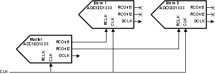 Figure 6-5 AutoSync Example
In order to synchronize the DCLK (and Data) outputs of multiple ADCs, the DCLKs must transition at the same time, as well as be in phase with one another. The DCLK at each ADC is generated from the CLK after some latency, plus tOD minus tAD. Therefore, in order for the DCLKs to transition at the same time, the CLK signal must reach each ADC at the same time. To tune out any differences in the CLK path to each ADC, the tAD adjust feature may be used. However, using the tAD adjust feature will also affect when the DCLK is produced at the output. If the device is in Demux Mode, then there are four possible phases which each DCLK may be generated on because the typical CLK = 1.8 GHz and DCLK = 450 MHz for this case. The RCLK signal controls the phase of the DCLK, so that each Slave DCLK is on the same phase as the Master DCLK.
The AutoSync feature may only be used via the Control Registers. For more information, see SNAA073.
6.1.4.2 DCLK Reset Feature
The DCLK reset feature is available via ECM, but it is disabled by default. DCLKI and DCLKQ are always synchronized, by design, and do not require a pulse from DCLK_RST to become synchronized.
The DCLK_RST signal must observe certain timing requirements, which are shown in Figure 4-6 of the Timing Diagrams. The DCLK_RST pulse must be of a minimum width and its deassertion edge must observe setup and hold times with respect to the CLK input rising edge. These timing specifications are listed as tPWR, tSR and tHR and may be found in Section 4.13.
The DCLK_RST signal can be asserted asynchronously to the input clock. If DCLK_RST is asserted, the DCLK output is held in a designated state (logic-high) in Demux Mode; in Non-Demux Mode, the DCLK continues to function normally. Depending upon when the DCLK_RST signal is asserted, there may be a narrow pulse on the DCLK line during this reset event. When the DCLK_RST signal is de-asserted, there are tSYNC_DLY CLK cycles of systematic delay and the next CLK rising edge synchronizes the DCLK output with those of other ADC12D1800RFs in the system. For 90° Mode (DDRPh = logic-high), the synchronizing edge occurs on the rising edge of CLK, 4 cycles after the first rising edge of CLK after DCLK_RST is released. For 0° Mode (DDRPh = logic-low), this is 5 cycles instead. The DCLK output is enabled again after a constant delay of tOD.
For both Demux and Non-Demux Modes, there is some uncertainty about how DCLK comes out of the reset state for the first DCLK_RST pulse. For the second (and subsequent) DCLK_RST pulses, the DCLK will come out of the reset state in a known way. Therefore, if using the DCLK Reset feature, it is recommended to apply one "dummy" DCLK_RST pulse before using the second DCLK_RST pulse to synchronize the outputs. This recommendation applies each time the device or channel is powered-on.
When using DCLK_RST to synchronize multiple ADC12D1800RFs, it is required that the Select Phase bits in the Control Register (Addr: Eh, Bits 3,4) be the same for each Master ADC12D1800RF.
6.1.5 Recommended System Chips
TI recommends these other chips including temperature sensors, clocking devices, and amplifiers in order to support the ADC12D1800RF in a system design.
6.1.5.1 Temperature Sensor
The ADC12D1800RF has an on-die temperature diode connected to pins Tdiode± which may be used to monitor the die temperature. TI also provides a family of temperature sensors for this application which monitor different numbers of external devices, see Table 6-3.
Table 6-3 Temperature Sensor Recommendation
| Number of External Devices Monitored | Recommended Temperature Sensor |
|---|---|
| 1 | LM95235 |
| 2 | LM95213 |
| 4 | LM95214 |
The temperature sensor (LM95235/13/14) is an 11-bit digital temperature sensor with a 2-wire System Management Bus (SMBus) interface that can monitor the temperature of one, two, or four remote diodes as well as its own temperature. It can be used to accurately monitor the temperature of up to one, two, or four external devices such as the ADC12D1800RF, a FPGA, other system components, and the ambient temperature.
The temperature sensor reports temperature in two different formats for +127.875°C/-128°C range and 0°/255°C range. It has a Sigma-Delta ADC core which provides the first level of noise immunity. For improved performance in a noisy environment, the temperature sensor includes programmable digital filters for Remote Diode temperature readings. When the digital filters are invoked, the resolution for the Remote Diode readings increases to 0.03125°C. For maximum flexibility and best accuracy, the temperature sensor includes offset registers that allow calibration for other types of diodes.
Diode fault detection circuitry in the temperature sensor can detect the absence or fault state of a remote diode: whether D+ is shorted to the power supply, D- or ground, or floating.
In the following typical application, the LM95213 is used to monitor the temperature of an ADC12D1800RF as well as an FPGA, see Figure 6-6. If this feature is unused, the Tdiode± pins may be left floating.
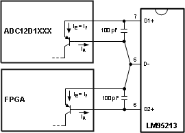 Figure 6-6 Typical Temperature Sensor Application
6.1.5.2 Clocking Device
The clock source can be a PLL/VCO device such as the LMX2531LQxxxx family of products. The specific device should be selected according to the desired ADC sampling clock frequency. The ADC12D1800RFRB uses the LMX2531LQ1778E, with the ADC clock source provided by the Aux PLL output. Other devices which may be considered based on clock source, jitter cleaning, and distribution purposes are the LMK01XXX, LMK02XXX, LMK03XXX and LMK04XXX product families.
6.1.5.3 Amplifiers for Analog Input
The following amplifiers can be used for ADC12D1800RF applications which require DC coupled input or signal gain, neither of which can be provided with a transformer coupled input circuit. In addition, several of the amplifiers provide single ended to differential conversion options:
Table 6-4 Amplifier Recommendation
| Amplifier | Bandwidth | Brief features |
|---|---|---|
| LMH3401 | 7 GHz | Fixed gain, single ended to differential conversion |
| LMH5401 | 8 GHz | Configurable Gain, single ended to differential conversion |
| LMH6401 | 4.5 GHz | Digital Variable Controlled Gain |
| LMH6554 | 2.8 GHz | Configurable gain |
| LMH6555 | 1.2 GHz | Fixed gain |
6.1.5.4 Balun Recommendations for Analog Input
The following baluns are recommended for the ADC12D1800RF for applications which require no gain. When evaluating a balun for the application of driving an ADC, some important qualities to consider are phase error and magnitude error.
Table 6-5 Balun Recommendations
| Balun | Bandwidth |
|---|---|
| Mini-Circuits TC1-1-13MA+ | 4.5 - 3000 MHz |
| Anaren B0430J50100A00 | 400 - 3000 MHz |
| Mini-Circuits ADTL2-18 | 30 - 1800 MHz |
6.2 Typical Application
6.2.1 RF Sampling Receiver
The ADC12D1800RF can be used to directly sample a signal in the RF frequency range for downstream processing. The wide input bandwidth, buffered input, high sampling rate and make ADC12D1800RF ideal for RF sampling applications.
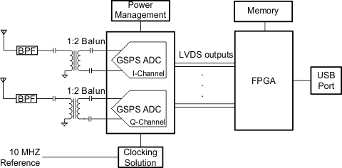 Figure 6-7 Simplified Schematic
6.2.2 Design Requirements
In this example ADC12D1800RF will be used to sample signals in DES mode and Non-Des mode. The design parameters are listed in Table 6-6.
Table 6-6 Design Requirements
| Design Parameters | Example Values (Non-DESI Mode) | Example Values (DESI Mode) |
|---|---|---|
| Signal center frequency | 2000 MHz | 1125 MHz |
| Signal bandwidth | 100 MHz | 400 MHz |
| ADC sampling rate | 1800 MSPS | 3600 MSPS |
| Signal nominal amplitude | –7 dBm | –7 dBm |
| Signal maximum amplitude | 6 dBm | 6 dBm |
| Minimum SNR (in BW of interest) | 47 dBc | 45 dBc |
| Minimum THD (in BW of interest) | –54 dBc | –58 dBc |
| Minimum SFDR (in BW of interest) | 56 dBc | 48 dBc |
6.2.3 Detailed Design Procedure
Use the step described below to design the RF receiver:
- Select the appropriate mode of operation (DES mode or Non-DES mode).
- Use the input signal frequency to select an appropriate sampling rate.
- Select the sampling rate so that the input signal is within the Nyquist zone and away from any harmonics and interleaving tones.
- Select the system components such as clocking device, amplifier for analog input and Balun according to sampling frequency and input signal frequency.
- See Section Section 6.1.5.2 for the recommended clock sources.
- See Table 6-4 for recommended analog amplifiers.
- See Table 6-5 for recommended Balun components.
- Select the bandpass filters and limiter components based on the requirement to attenuate the unwanted input signals.
6.2.4 Application Curves
The following curves show an RF signal at 1997.97 MHz captured at a sample rate of 1800 MSPS in NON-DES mode and an RF signal at 1123.97 MHz sample at an effective sample rate of 3600 MSPS in DES mode.
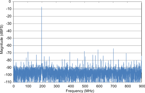
| NON-DES MODE | ||||
| Fin = 1997.97 MHz at –7 dBFS | ||||
| Fs = 1800 MSPS |
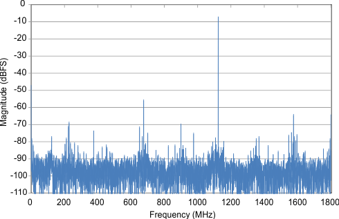
| DES MODE | ||||
| Fin = 1123.97 MHz at –7 dBFS | ||||
| Fs = 3600 MSPS |
Table 6-7 ADC12D1800RF Performance for Single Tone Signal at 1997.97 MHz in NON-DES Mode
| Parameter | Value |
|---|---|
| SNR | 47.6 dBc |
| SFDR | 56.7 dBc |
| THD | –54.9 dBc |
| SINAD | 46.9 dBc |
| ENOB | 7.5 bits |
Table 6-8 ADC12D1800RF Performance for Single Tone Signal at 1123.97 MHz in DES Mode
| Parameter | Value |
|---|---|
| SNR | 45.5 dBc |
| SFDR | 48.4 dBc |
| THD | –59.7 dBc |
| SINAD | 45.4 dBc |
| ENOB | 7.2 bits |