JAJSIL5A February   2020  – August 2020 ADC12DJ1600-Q1 , ADC12QJ1600-Q1 , ADC12SJ1600-Q1

PRODUCTION DATA  

  1. 特長
  2. アプリケーション
  3. 概要
  4. 概要 (続き)
  5. Revision History
  6. Device Comparison
  7. Pin Configuration and Functions
    1.     Pin Functions
  8. Specifications
    1. 8.1  Absolute Maximum Ratings
    2. 8.2  ESD Ratings
    3. 8.3  Recommended Operating Conditions
    4. 8.4  Thermal Information
    5. 8.5  Electrical Characteristics: DC Specifications
    6. 8.6  ADC12xJ1600-Q1: Electrical Characteristics: Power Consumption
    7. 8.7  ADC12xJ1600-Q1: Electrical Characteristics: AC Specifications
    8. 8.8  Timing Requirements
    9. 8.9  Switching Characteristics
    10. 8.10 Typical Characteristics
  9. Detailed Description
    1. 9.1 Overview
    2. 9.2 Functional Block Diagram
    3. 9.3 Feature Description
      1. 9.3.1 Analog Input
        1. 9.3.1.1 Analog Input Protection
        2. 9.3.1.2 Full-Scale Voltage (VFS) Adjustment
        3. 9.3.1.3 Analog Input Offset Adjust
        4. 9.3.1.4 ADC Core
          1. 9.3.1.4.1 ADC Theory of Operation
          2. 9.3.1.4.2 ADC Core Calibration
          3. 9.3.1.4.3 Analog Reference Voltage
          4. 9.3.1.4.4 ADC Over-range Detection
          5. 9.3.1.4.5 Code Error Rate (CER)
      2. 9.3.2 Temperature Monitoring Diode
      3. 9.3.3 Timestamp
      4. 9.3.4 Clocking
        1. 9.3.4.1 Converter PLL (C-PLL) for Sampling Clock Generation
        2. 9.3.4.2 LVDS Clock Outputs (PLLREFO±, TRIGOUT±)
        3. 9.3.4.3 Optional CMOS Clock Outputs (ORC, ORD)
        4. 9.3.4.4 SYSREF for JESD204C Subclass-1 Deterministic Latency
          1. 9.3.4.4.1 SYSREF Capture for Multi-Device Synchronization and Deterministic Latency
          2. 9.3.4.4.2 SYSREF Position Detector and Sampling Position Selection (SYSREF Windowing)
      5. 9.3.5 JESD204C Interface
        1. 9.3.5.1  Transport Layer
        2. 9.3.5.2  Scrambler
        3. 9.3.5.3  Link Layer
        4. 9.3.5.4  8B/10B Link Layer
          1. 9.3.5.4.1 Data Encoding (8B/10B)
          2. 9.3.5.4.2 Multiiframes and the Local Multiframe Clock (LMFC)
          3. 9.3.5.4.3 Code Group Synchronization (CGS)
          4. 9.3.5.4.4 Initial Lane Alignment Sequence (ILAS)
          5. 9.3.5.4.5 Frame and Multiframe Monitoring
        5. 9.3.5.5  64B/66B Link Layer
          1. 9.3.5.5.1 64B/66B Encoding
          2. 9.3.5.5.2 Multiblocks, Extended Multiblocks and the Local Extended Multiblock Clock (LEMC)
            1. 9.3.5.5.2.1 Block, Multiblock and Extended Multiblock Alignment using Sync Header
              1. 9.3.5.5.2.1.1 Cyclic Redundancy Check (CRC) Mode
              2. 9.3.5.5.2.1.2 Forward Error Correction (FEC) Mode
          3. 9.3.5.5.3 Initial Lane Alignment
          4. 9.3.5.5.4 Block, Multiblock and Extended Multiblock Alignment Monitoring
        6. 9.3.5.6  Physical Layer
          1. 9.3.5.6.1 SerDes Pre-Emphasis
        7. 9.3.5.7  JESD204C Enable
        8. 9.3.5.8  Multi-Device Synchronization and Deterministic Latency
        9. 9.3.5.9  Operation in Subclass 0 Systems
        10. 9.3.5.10 Alarm Monitoring
          1. 9.3.5.10.1 Clock Upset Detection
          2. 9.3.5.10.2 FIFO Upset Detection
    4. 9.4 Device Functional Modes
      1. 9.4.1 Low Power Mode and High Performance Mode
      2. 9.4.2 JESD204C Modes
        1. 9.4.2.1 JESD204C Transport Layer Data Formats
        2. 9.4.2.2 64B/66B Sync Header Stream Configuration
        3. 9.4.2.3 Redundant Data Mode (Alternate Lanes)
      3. 9.4.3 Power-Down Modes
      4. 9.4.4 Test Modes
        1. 9.4.4.1 Serializer Test-Mode Details
        2. 9.4.4.2 PRBS Test Modes
        3. 9.4.4.3 Clock Pattern Mode
        4. 9.4.4.4 Ramp Test Mode
        5. 9.4.4.5 Short and Long Transport Test Mode
          1. 9.4.4.5.1 Short Transport Test Pattern
        6. 9.4.4.6 D21.5 Test Mode
        7. 9.4.4.7 K28.5 Test Mode
        8. 9.4.4.8 Repeated ILA Test Mode
        9. 9.4.4.9 Modified RPAT Test Mode
      5. 9.4.5 Calibration Modes and Trimming
        1. 9.4.5.1 Foreground Calibration Mode
        2. 9.4.5.2 Background Calibration Mode
        3. 9.4.5.3 Low-Power Background Calibration (LPBG) Mode
      6. 9.4.6 Offset Calibration
      7. 9.4.7 Trimming
    5. 9.5 Programming
      1. 9.5.1 Using the Serial Interface
      2. 9.5.2 SCS
      3. 9.5.3 SCLK
      4. 9.5.4 SDI
      5. 9.5.5 SDO
      6. 9.5.6 Streaming Mode
      7. 9.5.7 SPI_Register_Map Registers
  10. 10Application and Implementation
    1. 10.1 Application Information
    2. 10.2 Typical Applications
      1. 10.2.1 Light Detection and Ranging (LiDAR) Digitizer
        1. 10.2.1.1 Design Requirements
        2. 10.2.1.2 Detailed Design Procedure
          1. 10.2.1.2.1 Analog Front-End Requirements
          2. 10.2.1.2.2 Calculating Clock and SerDes Frequencies
        3. 10.2.1.3 Application Curves
    3. 10.3 Initialization Set Up
  11. 11Power Supply Recommendations
    1. 11.1 Power Sequencing
  12. 12Layout
    1. 12.1 Layout Guidelines
    2. 12.2 Layout Example
  13. 13Device and Documentation Support
    1. 13.1 Device Support
    2. 13.2 Receiving Notification of Documentation Updates
    3. 13.3 Support Resources
    4. 13.4 商標
    5. 13.5 静電気放電に関する注意事項
    6. 13.6 Glossary
  14. 14Mechanical, Packaging, and Orderable Information

パッケージ・オプション

メカニカル・データ(パッケージ|ピン)
サーマルパッド・メカニカル・データ
発注情報

SYSREF for JESD204C Subclass-1 Deterministic Latency

SYSREF is a system timing reference used for JESD204C subclass-1 implementations of deterministic latency. SYSREF is used to achieve deterministic latency and for multi-device synchronization. SYSREF must be captured by the correct device clock edge in order to achieve repeatable latency and synchronization. The device includes a SYSREF Windowing feature to ease the requirements on the external clocking circuits and to simplify the synchronization process. SYSREF Windowing replaces the traditional setup and hold times as these are no longer required when SYSREF Windowing is used. SYSREF can be implemented as a single pulse or as a periodic clock. In periodic implementations, SYSREF must be equal to, or an integer division of, the local multiframe clock frequency in 8B/10B encoding modes or the local extended multiblock clock frequency in 64B/66B encoding modes. Equation 7 is used to calculate valid SYSREF frequencies in 8B/10B encoding modes. In 64B/66B modes, the denominator changes to 66 × 32 × E × n, where E is the number of multiblocks in an extended multiblock.
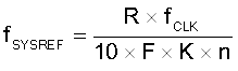
Equation 7. GUID-18A134B3-972C-4442-B934-BDA2AF04709B-low.gif

where