JAJSGV3B September 2015 – January 2019 ADC31JB68
PRODUCTION DATA.
- 1 特長
- 2 アプリケーション
- 3 概要
- 4 改訂履歴
- 5 概要(続き)
- 6 Pin Configuration and Functions
- 7 Specifications
- 8 Parameter Measurement Information
-
9 Detailed Description
- 9.1 Overview
- 9.2 Functional Block Diagram
- 9.3
Feature Description
- 9.3.1 Analog Inputs and Input Buffer
- 9.3.2 Amplitude and Phase Imbalance Correction
- 9.3.3 Over-Range Detection
- 9.3.4 Input Clock Divider
- 9.3.5 SYSREF Detection Gate
- 9.3.6 Serial Differential Output Drivers
- 9.3.7 ADC Core Calibration
- 9.3.8 Data Format
- 9.3.9 JESD204B Supported Features
- 9.3.10 JESD204B Interface
- 9.3.11 Transport Layer Configuration
- 9.3.12 Test Pattern Sequences
- 9.3.13 JESD204B Link Initialization
- 9.3.14 SPI
- 9.4 Device Functional Modes
- 9.5
Register Map
- 9.5.1
Register Descriptions
- 9.5.1.1 CONFIG_A (address = 0x0000) [reset = 0x3C]
- 9.5.1.2 DEVICE CONFIG (address = 0x0002) [reset = 0x00]
- 9.5.1.3 CHIP_TYPE (address = 0x0003 ) [reset = 0x03]
- 9.5.1.4 CHIP_ID (address = 0x0005, 0x0004) [reset = 0x00, 0x1B]
- 9.5.1.5 CHIP_VERSION (address =0x0006) [reset = 0x00]
- 9.5.1.6 VENDOR_ID (address = 0x000D, 0x000C) [reset = 0x04, 0x51]
- 9.5.1.7 SPI_CFG (address = 0x0010 ) [reset = 0x01]
- 9.5.1.8 OM1 (Operational Mode 1) (address = 0x0012) [reset = 0xC1]
- 9.5.1.9 OM2 (Operational Mode 2) (address = 0x0013) [reset = 0x20]
- 9.5.1.10 IMB_ADJ (Imbalance Adjust) (address = 0x0014) [reset = 0x00]
- 9.5.1.11 OVR_EN (Over-Range Enable) (address = 0x003A) [reset = 0x00]
- 9.5.1.12 OVR_HOLD (Over-Range Hold) (address = 0x003B) [reset = 0x00]
- 9.5.1.13 OVR_TH (Over-Range Threshold) (address = 0x003C) [reset = 0x00]
- 9.5.1.14 DC_MODE (DC Offset Correction Mode) (address = 0x003D) [reset = 0x00]
- 9.5.1.15 SER_CFG (Serial Lane Transmitter Configuration) (address = 0x0047) [reset = 0x00]
- 9.5.1.16 JESD_CTRL1 (JESD Configuration Control 1) (address = 0x0060) [reset = 0x7F]
- 9.5.1.17 JESD_CTRL2 (JESD Configuration Control 2) (address = 0x0061) [reset = 0x00]
- 9.5.1.18 JESD_RSTEP (JESD Ramp Pattern Step) (address = 0x0063, 0x0062) [reset = 0x00, 0x01]
- 9.5.1.19 SER_INV (Serial Lane Inversion Control) (address = 0x0064) [reset = 0x00]
- 9.5.1.20 JESD_STATUS (JESD Link Status) (address = 0x006C) [reset = N/A]
- 9.5.1
Register Descriptions
- 10Application and Implementation
- 11Power Supply Recommendations
- 12Layout
- 13デバイスおよびドキュメントのサポート
- 14メカニカル、パッケージ、および注文情報
パッケージ・オプション
メカニカル・データ(パッケージ|ピン)
- RTA|40
サーマルパッド・メカニカル・データ
- RTA|40
発注情報
9.3.2 Amplitude and Phase Imbalance Correction
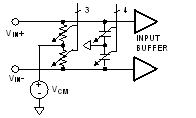
The ADC performance can be sensitive to amplitude and phase imbalance of the input differential signal. A front-end balance correction circuit is integrated to optimize the second-order distortion (HD2) performance of the ADC in the presence of an imbalanced input signal. 4-bit control of the phase mismatch and 3-bit control of the amplitude mismatch corrects the input mismatch before the input buffer. A simplified diagram of the amplitude and phase correction circuit at the ADC input is shown in Figure 30.
 Figure 30. Simplified Input Differential Balance Correction Circuit
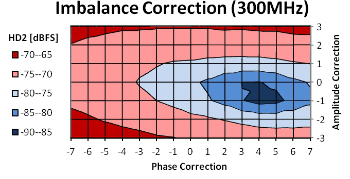
 Amplitude correction is achieved by varying the single-ended termination resistance of each input while maintaining constant total differential resistance, thereby adjusting the amplitude at each input but leaving the differential swing constant. Phase correction, also considered capacitive balance correction, varies the capacitive load at the ADC input, thereby counter-acting the phase difference between the analog inputs while minimally affecting amplitude. This function is useful for correcting the balance of transformers or filters that drive the ADC analog inputs. Figure 31 shows the measured HD2 resulting from an example 300-MHz imbalanced input signal measured over the available amplitude and phase correction settings. Performance parameters in the Converter Performance Characteristics are characterized with the amplitude and phase correction settings in the default condition (no correction).
 Figure 31. HD2 Optimization at 300 MHz Using Gain and Phase Imbalance Correction