JAJSGV3B September   2015  – January 2019 ADC31JB68

PRODUCTION DATA.  

  1. 特長
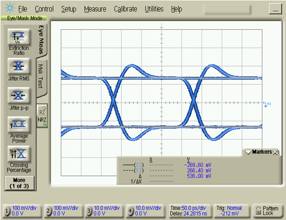
    1. 18 インチ / 5mil のFR4 マイクロストリップ・トレース出力の送信アイ、5Gb/s 時、ディエンファシスを最適化済み
  2. アプリケーション
  3. 概要
    1.     -1dBFS、450MHz 入力でのスペクトル
  4. 改訂履歴
  5. 概要(続き)
  6. Pin Configuration and Functions
    1.     Pin Functions
  7. Specifications
    1. 7.1 Absolute Maximum Ratings
    2. 7.2 ESD Ratings
    3. 7.3 Recommended Operating Conditions
    4. 7.4 Thermal Information
    5. 7.5 Electrical Characteristics: Converter Performance
    6. 7.6 Electrical Characteristics: Power Supply
    7. 7.7 Electrical Characteristics: Interface
    8. 7.8 Timing Requirements
    9. 7.9 Typical Characteristics
  8. Parameter Measurement Information
    1. 8.1 Interface Circuits
  9. Detailed Description
    1. 9.1 Overview
    2. 9.2 Functional Block Diagram
    3. 9.3 Feature Description
      1. 9.3.1  Analog Inputs and Input Buffer
      2. 9.3.2  Amplitude and Phase Imbalance Correction
      3. 9.3.3  Over-Range Detection
      4. 9.3.4  Input Clock Divider
      5. 9.3.5  SYSREF Detection Gate
      6. 9.3.6  Serial Differential Output Drivers
        1. 9.3.6.1 De-Emphasis Equalization
        2. 9.3.6.2 Serial Lane Inversion
      7. 9.3.7  ADC Core Calibration
      8. 9.3.8  Data Format
      9. 9.3.9  JESD204B Supported Features
      10. 9.3.10 JESD204B Interface
      11. 9.3.11 Transport Layer Configuration
        1. 9.3.11.1 Lane Configuration
        2. 9.3.11.2 Frame Format
        3. 9.3.11.3 ILA Information
      12. 9.3.12 Test Pattern Sequences
      13. 9.3.13 JESD204B Link Initialization
        1. 9.3.13.1 Frame Alignment
        2. 9.3.13.2 Code Group Synchronization
      14. 9.3.14 SPI
    4. 9.4 Device Functional Modes
      1. 9.4.1 Power-Down and Sleep Modes
    5. 9.5 Register Map
      1. 9.5.1 Register Descriptions
        1. 9.5.1.1  CONFIG_A (address = 0x0000) [reset = 0x3C]
          1. Table 6. CONFIG_A
        2. 9.5.1.2  DEVICE CONFIG (address = 0x0002) [reset = 0x00]
          1. Table 7. DEVICE CONFIG
        3. 9.5.1.3  CHIP_TYPE (address = 0x0003 ) [reset = 0x03]
          1. Table 8. CHIP_TYPE
        4. 9.5.1.4  CHIP_ID (address = 0x0005, 0x0004) [reset = 0x00, 0x1B]
          1. Table 9. CHIP_ID
        5. 9.5.1.5  CHIP_VERSION (address =0x0006) [reset = 0x00]
          1. Table 10. CHIP_VERSION
        6. 9.5.1.6  VENDOR_ID (address = 0x000D, 0x000C) [reset = 0x04, 0x51]
          1. Table 11. VENDOR_ID
        7. 9.5.1.7  SPI_CFG (address = 0x0010 ) [reset = 0x01]
          1. Table 12. SPI_CFG
        8. 9.5.1.8  OM1 (Operational Mode 1) (address = 0x0012) [reset = 0xC1]
          1. Table 13. OM1 (Operational Mode 1)
        9. 9.5.1.9  OM2 (Operational Mode 2) (address = 0x0013) [reset = 0x20]
          1. Table 14. OM2 (Operational Mode 2)
        10. 9.5.1.10 IMB_ADJ (Imbalance Adjust) (address = 0x0014) [reset = 0x00]
          1. Table 15. IMB_ADJ (Imbalance Adjust)
        11. 9.5.1.11 OVR_EN (Over-Range Enable) (address = 0x003A) [reset = 0x00]
          1. Table 16. OVR_EN (Over-Range Enable)
        12. 9.5.1.12 OVR_HOLD (Over-Range Hold) (address = 0x003B) [reset = 0x00]
          1. Table 17. OVR_HOLD (Over-Range Hold)
        13. 9.5.1.13 OVR_TH (Over-Range Threshold) (address = 0x003C) [reset = 0x00]
          1. Table 18. OVR_TH (Over-Range Threshold)
        14. 9.5.1.14 DC_MODE (DC Offset Correction Mode) (address = 0x003D) [reset = 0x00]
          1. Table 19. DC_MODE (DC Offset Correction Mode)
        15. 9.5.1.15 SER_CFG (Serial Lane Transmitter Configuration) (address = 0x0047) [reset = 0x00]
          1. Table 20. SER_CFG (Serial Lane Transmitter Configuration)
        16. 9.5.1.16 JESD_CTRL1 (JESD Configuration Control 1) (address = 0x0060) [reset = 0x7F]
          1. Table 21. JESD_CTRL1 (JESD Configuration Control 1)
        17. 9.5.1.17 JESD_CTRL2 (JESD Configuration Control 2) (address = 0x0061) [reset = 0x00]
          1. Table 22. JESD_CTRL2 (JESD Configuration Control 2)
        18. 9.5.1.18 JESD_RSTEP (JESD Ramp Pattern Step) (address = 0x0063, 0x0062) [reset = 0x00, 0x01]
          1. Table 23. JESD_RSTEP (JESD Ramp Pattern Step)
        19. 9.5.1.19 SER_INV (Serial Lane Inversion Control) (address = 0x0064) [reset = 0x00]
          1. Table 24. SER_INV (Serial Lane Inversion Control)
        20. 9.5.1.20 JESD_STATUS (JESD Link Status) (address = 0x006C) [reset = N/A]
          1. Table 25. JESD_STATUS (JESD Link Status)
  10. 10Application and Implementation
    1. 10.1 Application Information
      1. 10.1.1 Optimizing Converter Performance
        1. 10.1.1.1 Internal Noise Sources
        2. 10.1.1.2 External Noise Sources
      2. 10.1.2 Analog Input Considerations
        1. 10.1.2.1 Differential Analog Inputs and Full Scale Range
        2. 10.1.2.2 Analog Input Network Model
        3. 10.1.2.3 Input Bandwidth
        4. 10.1.2.4 Driving the Analog Input
        5. 10.1.2.5 Clipping and Over-Range
      3. 10.1.3 CLKIN, SYSREF, and SYNCb Input Considerations
        1. 10.1.3.1 Driving the CLKIN+ and CLKIN– Input
        2. 10.1.3.2 Driving the SYSREF Input
        3. 10.1.3.3 SYSREF Signaling
        4. 10.1.3.4 SYSREF Timing
        5. 10.1.3.5 Effectively Using the Detection Gate Feature
        6. 10.1.3.6 Driving the SYNCb Input
      4. 10.1.4 Output Serial Interface Considerations
        1. 10.1.4.1 Output Serial-Lane Interface
        2. 10.1.4.2 Voltage Swing and De-Emphasis Optimization
        3. 10.1.4.3 Minimizing EMI
      5. 10.1.5 JESD204B System Considerations
        1. 10.1.5.1 Frame and LMFC Clock Alignment Procedure
        2. 10.1.5.2 Link Interruption
        3. 10.1.5.3 Clock Configuration Examples
      6. 10.1.6 SPI
    2. 10.2 Typical Application
      1. 10.2.1 Design Requirements
      2. 10.2.2 Design Procedure
      3. 10.2.3 Application Curve
  11. 11Power Supply Recommendations
    1. 11.1 Power Supply Design
    2. 11.2 Decoupling
  12. 12Layout
    1. 12.1 Layout Guidelines
    2. 12.2 Layout Example
  13. 13デバイスおよびドキュメントのサポート
    1. 13.1 関連資料
    2. 13.2 ドキュメントの更新通知を受け取る方法
    3. 13.3 コミュニティ・リソース
    4. 13.4 商標
    5. 13.5 静電気放電に関する注意事項
    6. 13.6 Glossary
  14. 14メカニカル、パッケージ、および注文情報

パッケージ・オプション

メカニカル・データ(パッケージ|ピン)
サーマルパッド・メカニカル・データ
発注情報

De-Emphasis Equalization

De-emphasis of the differential output is provided as a form of continuous-time linear equalization that imposes a high-pass frequency response onto the output signal to compensate for frequency-dependent attenuation as the signal propagates through the channel to the receiver. In the time-domain, the de-emphasis appears as the bit transition transient followed by an immediate reduction in the differential amplitude, as shown in Figure 32. The characteristic appearance of the waveform changes with differential amplitude and the magnitude of de-emphasis applied. The serial lane rate determines the available period of time during which the de-emphasis transient settles. However, the lane rate does not affect the settling behavior of the applied de-emphasis. The de-emphasis value is measured as the ratio (in units of [dB]) between the peak voltage after the signal transition to the settled voltage value in one bit period. The data rate for this measurement is 1 Gb/s to allow settling of the de-emphasis transient.
ADC31JB68 Deemphasis_waveform.pngFigure 32. De-emphasis of the Differential Output Signal