JAJSGV3B September 2015 – January 2019 ADC31JB68
PRODUCTION DATA.
- 1 特長
- 2 アプリケーション
- 3 概要
- 4 改訂履歴
- 5 概要(続き)
- 6 Pin Configuration and Functions
- 7 Specifications
- 8 Parameter Measurement Information
-
9 Detailed Description
- 9.1 Overview
- 9.2 Functional Block Diagram
- 9.3
Feature Description
- 9.3.1 Analog Inputs and Input Buffer
- 9.3.2 Amplitude and Phase Imbalance Correction
- 9.3.3 Over-Range Detection
- 9.3.4 Input Clock Divider
- 9.3.5 SYSREF Detection Gate
- 9.3.6 Serial Differential Output Drivers
- 9.3.7 ADC Core Calibration
- 9.3.8 Data Format
- 9.3.9 JESD204B Supported Features
- 9.3.10 JESD204B Interface
- 9.3.11 Transport Layer Configuration
- 9.3.12 Test Pattern Sequences
- 9.3.13 JESD204B Link Initialization
- 9.3.14 SPI
- 9.4 Device Functional Modes
- 9.5
Register Map
- 9.5.1
Register Descriptions
- 9.5.1.1 CONFIG_A (address = 0x0000) [reset = 0x3C]
- 9.5.1.2 DEVICE CONFIG (address = 0x0002) [reset = 0x00]
- 9.5.1.3 CHIP_TYPE (address = 0x0003 ) [reset = 0x03]
- 9.5.1.4 CHIP_ID (address = 0x0005, 0x0004) [reset = 0x00, 0x1B]
- 9.5.1.5 CHIP_VERSION (address =0x0006) [reset = 0x00]
- 9.5.1.6 VENDOR_ID (address = 0x000D, 0x000C) [reset = 0x04, 0x51]
- 9.5.1.7 SPI_CFG (address = 0x0010 ) [reset = 0x01]
- 9.5.1.8 OM1 (Operational Mode 1) (address = 0x0012) [reset = 0xC1]
- 9.5.1.9 OM2 (Operational Mode 2) (address = 0x0013) [reset = 0x20]
- 9.5.1.10 IMB_ADJ (Imbalance Adjust) (address = 0x0014) [reset = 0x00]
- 9.5.1.11 OVR_EN (Over-Range Enable) (address = 0x003A) [reset = 0x00]
- 9.5.1.12 OVR_HOLD (Over-Range Hold) (address = 0x003B) [reset = 0x00]
- 9.5.1.13 OVR_TH (Over-Range Threshold) (address = 0x003C) [reset = 0x00]
- 9.5.1.14 DC_MODE (DC Offset Correction Mode) (address = 0x003D) [reset = 0x00]
- 9.5.1.15 SER_CFG (Serial Lane Transmitter Configuration) (address = 0x0047) [reset = 0x00]
- 9.5.1.16 JESD_CTRL1 (JESD Configuration Control 1) (address = 0x0060) [reset = 0x7F]
- 9.5.1.17 JESD_CTRL2 (JESD Configuration Control 2) (address = 0x0061) [reset = 0x00]
- 9.5.1.18 JESD_RSTEP (JESD Ramp Pattern Step) (address = 0x0063, 0x0062) [reset = 0x00, 0x01]
- 9.5.1.19 SER_INV (Serial Lane Inversion Control) (address = 0x0064) [reset = 0x00]
- 9.5.1.20 JESD_STATUS (JESD Link Status) (address = 0x006C) [reset = N/A]
- 9.5.1
Register Descriptions
- 10Application and Implementation
- 11Power Supply Recommendations
- 12Layout
- 13デバイスおよびドキュメントのサポート
- 14メカニカル、パッケージ、および注文情報
パッケージ・オプション
メカニカル・データ(パッケージ|ピン)
- RTA|40
サーマルパッド・メカニカル・データ
- RTA|40
発注情報
10.1.2.1 Differential Analog Inputs and Full Scale Range
The ADC31JB68 device has one channel with a pair of analog signal input pins: VIN+, VIN−. VIN, the input differential signal for a channel, is defined as VIN = (VIN+) – (VIN−). Table 26 shows the expected input signal range when the differential signal swings about the input common mode voltage, VCM. The full-scale differential peak-to-peak input range is equal to twice the internal reference voltage, VREF. Nominally, the full scale range is 1.7 Vpp-diff, therefore the maximum peak-to-peak single-ended voltage is 0.85 Vpp at each of the VIN+ and VIN− pins.
The single-ended signals must be opposite in polarity relative to the VCM voltage to provide a purely differential signal, otherwise the common-mode component may be rejected by the ADC input. Table 26 indicates the input to output relationship of the ADC31JB68 device where VREF = 0.85 V.
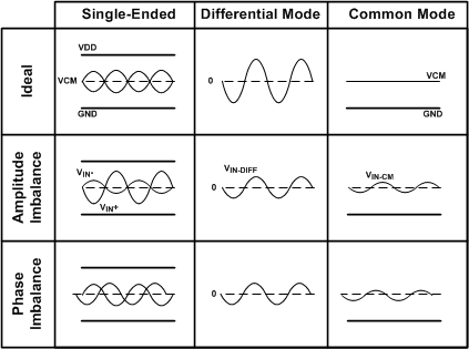
Differential signals with amplitude or phase imbalances result in lower system performance compared to perfectly balanced signals. Imbalances in signal path circuits lead to differential-to-common-mode signal conversion and differential signal amplitude loss as shown in Figure 60. This deviation or imbalance directly causes a reduction in the signal amplitude and may also lead to distortion, particularly even order harmonic distortion, as the signal propagates through the signal path. The Amplitude and Phase Imbalance Correction feature in the ADC31JB68 helps to correct amplitude or phase errors of the signal.
Table 26. Mapping of the Analog Input Full Scale Range to Digital Codes
| VIN+ | VIN– | 2s Complement Output | Binary Output | Note |
|---|---|---|---|---|
| VCM + VREF / 2 | VCM – VREF / 2 | 0111 1111 1111 1111 | 1111 1111 1111 1111 | Positive full-scale |
| VCM + VREF / 4 | VCM – VREF / 4 | 0100 0000 0000 0000 | 1100 0000 0000 0000 | |
| VCM | VCM | 0000 0000 0000 0000 | 1000 0000 0000 0000 | Mid-scale |
| VCM – VREF / 4 | VCM + VREF / 4 | 1100 0000 0000 0000 | 0100 0000 0000 0000 | |
| VCM – VREF / 2 | VCM + VREF / 2 | 1000 0000 0000 0000 | 0000 0000 0000 0000 | Negative full-scale |
 Figure 60. Differential Signal Waveform and Signal Imbalance