JAJSCS3C May 2016 – December 2016 ADC32RF45
PRODUCTION DATA.
- 1 特長
- 2 アプリケーション
- 3 概要
- 4 改訂履歴
- 5 Pin Configuration and Functions
- 6 Specifications
- 7 Parameter Measurement Information
-
8 Detailed Description
- 8.1 Overview
- 8.2 Functional Block Diagram
- 8.3
Feature Description
- 8.3.1 Analog Inputs
- 8.3.2 Clock Input
- 8.3.3 SYSREF Input
- 8.3.4 DDC Block
- 8.3.5 NCO Switching
- 8.3.6 SerDes Transmitter Interface
- 8.3.7 Eye Diagrams
- 8.3.8 Alarm Outputs: Power Detectors for AGC Support
- 8.3.9 Power-Down Mode
- 8.3.10 ADC Test Pattern
- 8.4
Device Functional Modes
- 8.4.1 Device Configuration
- 8.4.2
JESD204B Interface
- 8.4.2.1 JESD204B Initial Lane Alignment (ILA)
- 8.4.2.2 JESD204B Frame Assembly
- 8.4.2.3 JESD204B Frame Assembly in Bypass Mode
- 8.4.2.4 JESD204B Frame Assembly with Decimation (Single-Band DDC): Complex Output
- 8.4.2.5 JESD204B Frame Assembly with Decimation (Single-Band DDC): Real Output
- 8.4.2.6 JESD204B Frame Assembly with Decimation (Single-Band DDC): Real Output
- 8.4.2.7 JESD204B Frame Assembly with Decimation (Dual-Band DDC): Complex Output
- 8.4.2.8 JESD204B Frame Assembly with Decimation (Dual-Band DDC): Real Output
- 8.4.3 Serial Interface
- 8.5
Register Maps
- 8.5.1 Example Register Writes
- 8.5.2
Register Descriptions
- 8.5.2.1
General Registers
- 8.5.2.1.1 Register 000h (address = 000h), General Registers
- 8.5.2.1.2 Register 002h (address = 002h), General Registers
- 8.5.2.1.3 Register 003h (address = 003h), General Registers
- 8.5.2.1.4 Register 004h (address = 004h), General Registers
- 8.5.2.1.5 Register 010h (address = 010h), General Registers
- 8.5.2.1.6 Register 011h (address = 011h), General Registers
- 8.5.2.1.7 Register 012h (address = 012h), General Registers
- 8.5.2.1
General Registers
- 8.5.3
Master Page (M = 0)
- 8.5.3.1 Register 020h (address = 020h), Master Page
- 8.5.3.2 Register 032h (address = 032h), Master Page
- 8.5.3.3 Register 039h (address = 039h), Master Page
- 8.5.3.4 Register 03Ch (address = 03Ch), Master Page
- 8.5.3.5 Register 05Ah (address = 05Ah), Master Page
- 8.5.3.6 Register 03Dh (address = 3Dh), Master Page
- 8.5.3.7 Register 057h (address = 057h), Master Page
- 8.5.3.8 Register 058h (address = 058h), Master Page
- 8.5.4 ADC Page (FFh, M = 0)
- 8.5.5 Digital Function Page (610000h, M = 1 for Channel A and 610100h, M = 1 for Channel B)
- 8.5.6 Offset Corr Page Channel A (610000h, M = 1)
- 8.5.7 Offset Corr Page Channel B (610000h, M = 1)
- 8.5.8 Digital Gain Page (610005h, M = 1 for Channel A and 610105h, M = 1 for Channel B)
- 8.5.9 Main Digital Page Channel A (680000h, M = 1)
- 8.5.10 Main Digital Page Channel B (680001h, M = 1)
- 8.5.11
JESD Digital Page (6900h, M = 1)
- 8.5.11.1 Register 001h (address = 001h), JESD Digital Page
- 8.5.11.2 Register 002h (address = 002h ), JESD Digital Page
- 8.5.11.3 Register 003h (address = 003h), JESD Digital Page
- 8.5.11.4 Register 004h (address = 004h), JESD Digital Page
- 8.5.11.5 Register 006h (address = 006h), JESD Digital Page
- 8.5.11.6 Register 007h (address = 007h), JESD Digital Page
- 8.5.11.7 Register 016h (address = 016h), JESD Digital Page
- 8.5.11.8 Register 017h (address = 017h), JESD Digital Page
- 8.5.11.9 Register 032h-035h (address = 032h-035h), JESD Digital Page
- 8.5.11.10 Register 036h (address = 036h), JESD Digital Page
- 8.5.11.11 Register 037h (address = 037h), JESD Digital Page
- 8.5.11.12 Register 03Eh (address = 03Eh), JESD Digital Page
- 8.5.12
Decimation Filter Page
- 8.5.12.1 Register 000h (address = 000h), Decimation Filter Page
- 8.5.12.2 Register 001h (address = 001h), Decimation Filter Page
- 8.5.12.3 Register 002h (address = 2h), Decimation Filter Page
- 8.5.12.4 Register 005h (address = 005h), Decimation Filter Page
- 8.5.12.5 Register 006h (address = 006h), Decimation Filter Page
- 8.5.12.6 Register 007h (address = 007h), Decimation Filter Page
- 8.5.12.7 Register 008h (address = 008h), Decimation Filter Page
- 8.5.12.8 Register 009h (address = 009h), Decimation Filter Page
- 8.5.12.9 Register 00Ah (address = 00Ah), Decimation Filter Page
- 8.5.12.10 Register 00Bh (address = 00Bh), Decimation Filter Page
- 8.5.12.11 Register 00Ch (address = 00Ch), Decimation Filter Page
- 8.5.12.12 Register 00Dh (address = 00Dh), Decimation Filter Page
- 8.5.12.13 Register 00Eh (address = 00Eh), Decimation Filter Page
- 8.5.12.14 Register 00Fh (address = 00Fh), Decimation Filter Page
- 8.5.12.15 Register 010h (address = 010h), Decimation Filter Page
- 8.5.12.16 Register 011h (address = 011h), Decimation Filter Page
- 8.5.12.17 Register 014h (address = 014h), Decimation Filter Page
- 8.5.12.18 Register 016h (address = 016h), Decimation Filter Page
- 8.5.12.19 Register 01Eh (address = 01Eh), Decimation Filter Page
- 8.5.12.20 Register 01Fh (address = 01Fh), Decimation Filter Page
- 8.5.12.21 Register 033h-036h (address = 033h-036h), Decimation Filter Page
- 8.5.12.22 Register 037h (address = 037h), Decimation Filter Page
- 8.5.12.23 Register 03Ah (address = 03Ah), Decimation Filter Page
- 8.5.13
Power Detector Page
- 8.5.13.1 Register 000h (address = 000h), Power Detector Page
- 8.5.13.2 Register 001h-002h (address = 001h-002h), Power Detector Page
- 8.5.13.3 Register 003h (address = 003h), Power Detector Page
- 8.5.13.4 Register 007h-00Ah (address = 007h-00Ah), Power Detector Page
- 8.5.13.5 Register 00Bh-00Ch (address = 00Bh-00Ch), Power Detector Page
- 8.5.13.6 Register 00Dh (address = 00Dh), Power Detector Page
- 8.5.13.7 Register 00Eh (address = 00Eh), Power Detector Page
- 8.5.13.8 Register 00Fh, 010h-012h, and 016h-019h (address = 00Fh, 010h-012h, and 016h-019h), Power Detector Page
- 8.5.13.9 Register 013h-01Ah (address = 013h-01Ah), Power Detector Page
- 8.5.13.10 Register 01Dh-01Eh (address = 01Dh-01Eh), Power Detector Page
- 8.5.13.11 Register 020h (address = 020h), Power Detector Page
- 8.5.13.12 Register 021h (address = 021h), Power Detector Page
- 8.5.13.13 Register 022h-025h (address = 022h-025h), Power Detector Page
- 8.5.13.14 Register 027h (address = 027h), Power Detector Page
- 8.5.13.15 Register 02Bh (address = 02Bh), Power Detector Page
- 8.5.13.16 Register 032h-035h (address = 032h-035h), Power Detector Page
- 8.5.13.17 Register 037h (address = 037h), Power Detector Page
- 8.5.13.18 Register 038h (address = 038h), Power Detector Page
- 9 Application and Implementation
- 10Power Supply Recommendations
- 11Layout
- 12デバイスおよびドキュメントのサポート
- 13メカニカル、パッケージ、および注文情報
9 Application and Implementation
NOTE
Information in the following applications sections is not part of the TI component specification, and TI does not warrant its accuracy or completeness. TI’s customers are responsible for determining suitability of components for their purposes. Customers should validate and test their design implementation to confirm system functionality.
9.1 Application Information
9.1.1 Start-Up Sequence
The steps in Table 115 are recommended as the power-up sequence when the ADC32RF45 is in bypass mode with a 12-bit output (LMFS = 82820).
Table 115. Initialization Sequence
| STEP | DESCRIPTION | PAGE, REGISTER ADDRESS AND DATA | COMMENT |
|---|---|---|---|
| 1 | Supply all supply voltages. There is no required power-supply sequence for the 1.15 V, 1.2 V, and 1.9 V supplies, and can be supplied in any order. | — | — |
| 2 | Provide the SYSREF signal. | — | — |
| 3 | Pulse a hardware reset (low-to-high-to-low) on pins 33 and 34. | — | — |
| 4 | Write the register addresses described in the PowerUpConfig file. | See the files located in SBAA226 | The Power-up config file contains analog trim registers that are required for best performance of the ADC. Write these registers every time after power up. |
| 5 | Write the register addresses mentioned in the ILConfigNyqX_ChA file, where X is the Nyquist zone. | See the files located in SBAA226 | Based on the signal band of interest, provide the Nyquist zone information to the device. |
| 6 | Write the register addresses mentioned in the ILConfigNyqX_ChB file, where X is the Nyquist zone. | See the files located in SBAA226 | This step optimizes device’ performance by reducing interleaving mismatch errors. |
| 6.1 | Wait for 50 ms for the device to estimate the interleaving errors. | — | — |
| 7 | Depending upon the Nyquist band of operation, choose and write the registers from the appropriate file, NLConfigNyqX_ChA, where X is the Nyquist zone. | See the files located in SBAA226 | Third-order nonlinearity of the device is optimized by this step for channel A. |
| 7.1 | Depending upon the Nyquist band of operation, choose and write the registers from the appropriate file, NLConfigNyqX_ChB, where X is the Nyquist zone. | See the files located in SBAA226 | Third-order nonlinearity of the device is optimized by this step for channel B. |
| 8 | Configure the JESD interface and DDC block by writing the registers mentioned in the DDC Config file. | See the files located in SBAA226 | Determine the DDC and JESD interface LMFS options. Program these options in this step. |
9.1.2 Hardware Reset
Timing information for the hardware reset is shown in Figure 230 and Table 116.
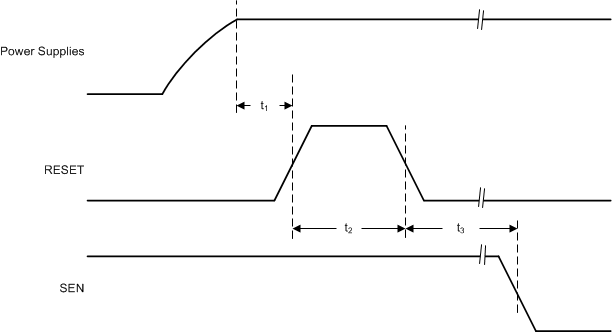 Figure 230. Hardware Reset Timing Diagram
Table 116. Hardware Reset Timing Information
| MIN | TYP | MAX | UNIT | ||
|---|---|---|---|---|---|
| t1 | Power-on delay from power-up to active high RESET pulse | 1 | ms | ||
| t2 | Reset pulse duration: active high RESET pulse duration | 1 | µs | ||
| t3 | Register write delay from RESET disable to SEN active | 100 | ns | ||
9.1.3 SNR and Clock Jitter
The signal-to-noise ratio (SNR) of the ADC is limited by three different factors: quantization noise, thermal noise, and jitter, as shown in Equation 5. The quantization noise is typically not noticeable in pipeline converters and is 84 dB for a 14-bit ADC. The thermal noise limits the SNR at low input frequencies and the clock jitter sets the SNR for higher input frequencies.

The SNR limitation resulting from sample clock jitter can be calculated by Equation 6:

The total clock jitter (TJitter) has two components: the internal aperture jitter (90 fS) is set by the noise of the clock input buffer and the external clock jitter. TJitter can be calculated by Equation 7:

External clock jitter can be minimized by using high-quality clock sources and jitter cleaners as well as band-pass filters at the clock input. A faster clock slew rate also improves the ADC aperture jitter.
The ADC32RF45 has a thermal noise of approximately 63 dBFS and an internal aperture jitter of 90 fS. The SNR, depending on the amount of external jitter for different input frequencies, is shown in Figure 231.
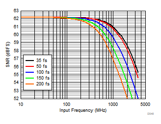 Figure 231. ADC SNR vs Input Frequency and External Clock Jitter
9.1.3.1 External Clock Phase Noise Consideration
External clock jitter can be calculated by integrating the phase noise of the clock source out to approximately two times of the ADC sampling rate (2 × fS), as shown in Figure 232. In order to maximize the ADC SNR, an external band-pass filter is recommended to be used on the clock input. This filter reduces the jitter contribution from the broadband clock phase noise floor by effectively reducing the integration bandwidth to the pass band of the band-pass filter. This method is suitable when estimating the overall ADC SNR resulting from clock jitter at a certain input frequency.
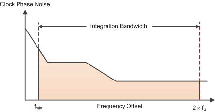 Figure 232. Integration Bandwidth for Extracting Jitter from Clock Phase Noise
However, when estimating the affect of a nearby blocker (such as a strong in-band interferer to the sensitivity, the phase noise information can be used directly to estimate the noise budget contribution at a certain offset frequency, as shown in Figure 233.
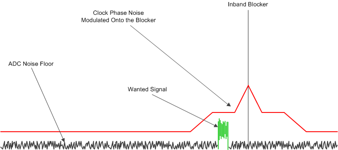 Figure 233. Small Wanted Signal in Presence of Interferer
At the sampling instant, the phase noise profile of the clock source convolves with the input signal (for example, the small wanted signal and the strong interferer merge together). If the power of the clock phase noise in the signal band of interest is too large, the wanted signal cannot not be recovered.
The resulting equivalent phase noise at the ADC input is also dependent on the sampling rate of the ADC and frequency of the input signal. The ADC sampling rate scales the clock phase noise, as shown in Equation 8.

Using this information, the noise contribution resulting from the phase noise profile of the ADC sampling clock can be calculated.
9.1.4 Power Consumption in Different Modes
The ADC32RF45 consumes approximately 6.6 W of power when both channels are active with a 12-bit, 3-GSPS output and a DDC option is not used (bypass mode). When different DDC options are used, the power consumption on the DVDD supply changes by a small amount but remains unaffected on other supplies. In the applications requiring just one channel to be active, channel A must be chosen as the active channel and channel B can be powered down. Power consumption reduces to approximately 4 W in single-channel operation with a 12-bit, 3-GSPS output (bypass mode).
Table 117 shows power consumption in different DDC modes for dual-channel and single-channel operation.
Table 117. Power Consumption in Different DDC Modes (Sampling Clock Frequency, fS = 3 GSPS)
| DECIMATION OPTION | ACTIVE CHANNEL |
ACTIVE DDC | AVDD19 (mA) | AVDD (mA) | DVDD (mA) | TOTAL POWER (mW) |
|---|---|---|---|---|---|---|
| Bypass mode | Channels A, B | NA | 1792 | 972 | 1748 | 6533 |
| Divide-by-4 | Channels A, B | Single | 1777 | 970 | 1785 | 6545 |
| Divide-by-8 | Channels A, B | Dual | 1777 | 973 | 1960 | 6749 |
| Divide-by-8 | Channels A, B | Single | 1777 | 973 | 1730 | 6485 |
| Divide-by-16 | Channels A, B | Dual | 1777 | 972 | 1971 | 6761 |
| Divide-by-16 | Channels A, B | Single | 1777 | 972 | 1705 | 6455 |
| Divide-by-24 | Channels A, B | Dual | 1771 | 975 | 1938 | 6715 |
| Divide-by-24 | Channels A, B | Single | 1771 | 972 | 1667 | 6400 |
| Divide-by-32 | Channels A, B | Dual | 1768 | 972 | 1835 | 6587 |
| Divide-by-32 | Channels A, B | Single | 1768 | 970 | 1574 | 6285 |
| Bypass mode | Channel A | NA | 968 | 793 | 1133 | 4054 |
| Divide-by-4 | Channel A | Single | 961 | 796 | 1096 | 4002 |
| Divide-by-8 | Channel A | Dual | 961 | 790 | 1168 | 4078 |
| Divide-by-8 | Channel A | Single | 961 | 786 | 1047 | 3934 |
| Divide-by-16 | Channel A | Dual | 961 | 789 | 1172 | 4081 |
| Divide-by-16 | Channel A | Single | 961 | 786 | 1045 | 3932 |
| Divide-by-24 | Channel A | Dual | 958 | 785 | 1155 | 4051 |
| Divide-by-24 | Channel A | Single | 958 | 787 | 1016 | 3894 |
| Divide-by-32 | Channel A | Dual | 956 | 788 | 1104 | 3992 |
| Divide-by-32 | Channel A | Single | 956 | 786 | 978 | 3845 |
9.1.5 Using DC Coupling in the ADC32RF45
The ADC32RF45 can be used in dc-coupling applications. However, the following points must be considered when designing the system:
- Ensure that the correct common-mode voltage is used at the ADC analog inputs.
- Ensure that the correct SPI settings are written to the ADC.
The analog inputs are internally self-biased to VCM through approximately a 33-Ω resistor. The internal biasing resistors also function as a termination resistor. However, if a different termination is required, the external resistor RTERM can be differentially placed between the analog inputs, as shown in Figure 234. The amplifier VOCM pin is recommended to be driven from the CM pin of the ADC to help the amplifier output common-mode voltage track the required common-mode voltage of the ADC.

As shown in Figure 235, the ADC32RF45 has a digital block that estimates and corrects the offset mismatch among four interleaving ADC cores for a given channel.
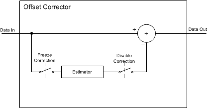 Figure 235. Offset Corrector in the ADC32RF45
The offset corrector block nullifies dc, fS / 8, fS / 4, 3 fS / 8, and fS / 2. The resulting spectrum becomes free from static spurs at these frequencies. The corrector continuously processes the data coming from the interleaving ADC cores and cannot distinguish if the tone at these frequencies is part of signal or if the tone originated from a mismatch among the interleaving ADC cores. Thus, in applications where the signal is present at these frequencies, the offset corrector block can be bypassed.
9.1.5.1 Bypassing the Offset Corrector Block
When the offset corrector is bypassed, offset mismatch among interleaving ADC cores appears in the ADC output spectrum. To correct the effects of mismatch, place the ADC in an idle channel state (no signal at the ADC inputs) and the corrector must be allowed to run for some time to estimate the mismatch, then the corrector is frozen so that the last estimated value is held. Required register writes are provided in Table 118.
Table 118. Freezing and Bypassing the Offset Corrector Block
| STEP | REGISTER WRITE | COMMENT |
|---|---|---|
| STEPS FOR FREEZING THE CORRECTOR BLOCK | ||
| 1 | — | Signal source is turned off. The device detects an idle channel at its input. |
| 2 | — | Wait for at least 0.4 ms for the corrector to estimate the internal offset |
| 3 | Address 4001h, value 00h | Select Offset Corr Page Channel A |
| Address 4002h, value 00h | ||
| Address 4003h, value 00h | ||
| Address 4004h, value 61h | ||
| Address 6068h, value C2h | Freeze the corrector for channel A | |
| Address 4003h, value 01h | Select Offset Corr Page Channel B | |
| Address 6068h, value C2h | Freeze the corrector for channel B | |
| 4 | — | Signal source can now be turned on |
| STEPS FOR BYPASSING THE CORRECTOR BLOCK | ||
| 1 | Address 4001h, value 00h | — |
| Address 4002h, value 00h | ||
| Address 4003h, value 00h | ||
| Address 4004h, value 61h | Select Offset Corr Page Channel A | |
| Address 6068h, value 46h | Disable the corrector for channel A | |
| Address 4003h, value 01h | Select Offset Corr Page Channel B | |
| Address 6068h, value 46h | Disable the corrector for channel B | |
9.1.5.1.1 Effect of Temperature
Figure 236 and Figure 237 show the behavior of nfS / 8 tones with respect to temperature when the offset corrector block is frozen or disabled.
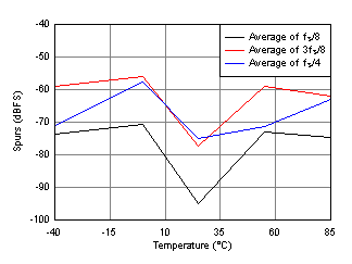 Figure 236. Offset Corrector Block Frozen at Room Temperature
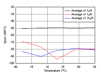 Figure 237. Offset Corrector Block Disabled
9.2 Typical Application
The ADC32RF45 is designed for wideband receiver applications demanding high dynamic range over a large input frequency range. A typical schematic for an ac-coupled receiver is shown in Figure 238.
Decoupling capacitors with low ESL are recommended to be placed as close as possible at the pins indicated in Figure 238. Additional capacitors can be placed on the remaining power pins.
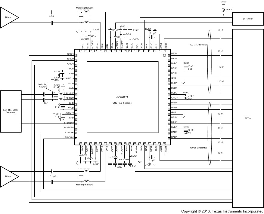 Figure 238. Typical Application Implementation Diagram
9.2.1 Design Requirements
9.2.1.1 Transformer-Coupled Circuits
Typical applications involving transformer-coupled circuits are discussed in this section. To ensure good amplitude and phase balance at the analog inputs, transformers (such as TC1-1-13 and TC1-1-43) can be used from the dc to 1000-MHz range and from the 1000-MHz to 4-GHz range of input frequencies, respectively. When designing the driving circuits, the ADC input impedance (or SDD11) must be considered.
By using the simple drive circuit of Figure 239, uniform performance can be obtained over a wide frequency range. The buffers present at the analog inputs of the device help isolate the external drive source from the switching currents of the sampling circuit.
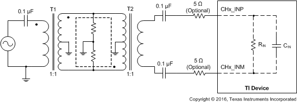 Figure 239. Input Drive Circuit
9.2.2 Detailed Design Procedure
For optimum performance, the analog inputs must be driven differentially. This architecture improves common-mode noise immunity and even-order harmonic rejection. A small resistor (5 Ω to 10 Ω) in series with each input pin is recommended to damp out ringing caused by package parasitics, as shown in Figure 239.
9.2.3 Application Curves
Figure 240 and Figure 241 show the typical performance at 100 MHz and 1780 MHz, respectively.
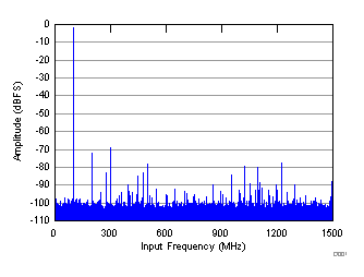
| SNR = 61.8 dBFS, SINAD = 61.2 dBFS, HD2 = 71 dBc, HD3 = 75 dBc, SFDR = 71 dBc, THD = 68 dBc, IL spur = 77 dBc, worst spur = 73 dBc |
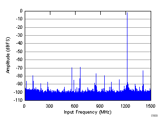
| SNR = 57.9 dBFS, SINAD = 57.1 dBFS, HD2 = 63 dBc, HD3 = 66 dBc, SFDR = 63 dBc, THD = 60 dBc, IL spur = 79 dBc, worst spur = 77 dBc |