JAJSGG2C October   2018  – June 2019 ADS125H02

PRODUCTION DATA.  

  1. 特長
  2. アプリケーション
  3. 概要
    1.     機能ブロック図
  4. 改訂履歴
  5. 概要(続き)
  6. Device Comparison Table
  7. Pin Configuration and Functions
    1.     Pin Functions
  8. Specifications
    1. 8.1 Absolute Maximum Ratings
    2. 8.2 ESD Ratings
    3. 8.3 Recommended Operating Conditions
    4. 8.4 Thermal Information
    5. 8.5 Electrical Characteristics
    6. 8.6 Timing Requirements
    7. 8.7 Switching Characteristics
    8. 8.8 Typical Characteristics
  9. Parameter Measurement Information
    1. 9.1 Noise Performance
  10. 10Detailed Description
    1. 10.1 Overview
    2. 10.2 Functional Block Diagram
    3. 10.3 Feature Description
      1. 10.3.1 Input Range
      2. 10.3.2 Analog Inputs
        1. 10.3.2.1 ESD Diodes
        2. 10.3.2.2 Input Multiplexer
          1. 10.3.2.2.1 Analog Inputs (AIN0, AIN1, AINCOM)
          2. 10.3.2.2.2 High-Voltage Power Supply Readback
          3. 10.3.2.2.3 Internal VCOM Connection (Default)
          4. 10.3.2.2.4 Temperature Sensor
      3. 10.3.3 Programmable Gain Amplifier (PGA)
        1. 10.3.3.1 PGA Operating Range
        2. 10.3.3.2 PGA Monitor
      4. 10.3.4 Reference Voltage
        1. 10.3.4.1 Internal Reference
        2. 10.3.4.2 External Reference
        3. 10.3.4.3 AVDD Power-Supply Reference
        4. 10.3.4.4 Reference Monitor
      5. 10.3.5 Current Sources (IDAC1 and IDAC2)
      6. 10.3.6 General-Purpose Inputs and Outputs (GPIOs)
      7. 10.3.7 ADC Modulator
      8. 10.3.8 Digital Filter
        1. 10.3.8.1 Sinc Filter Mode
          1. 10.3.8.1.1 Sinc Filter Frequency Response
        2. 10.3.8.2 FIR Filter
        3. 10.3.8.3 50-Hz and 60-Hz Normal Mode Rejection
    4. 10.4 Device Functional Modes
      1. 10.4.1 Conversion Control
        1. 10.4.1.1 Continuous-Conversion Mode
        2. 10.4.1.2 Pulse-Conversion Mode
        3. 10.4.1.3 Conversion Latency
        4. 10.4.1.4 Start-Conversion Delay
      2. 10.4.2 Auto-Zero Mode
      3. 10.4.3 Clock Mode
      4. 10.4.4 Reset
        1. 10.4.4.1 Power-On Reset
        2. 10.4.4.2 Reset by Pin
        3. 10.4.4.3 Reset by Command
      5. 10.4.5 Calibration
        1. 10.4.5.1 Offset and Full-Scale Calibration
          1. 10.4.5.1.1 Offset Calibration Registers
          2. 10.4.5.1.2 Full-Scale Calibration Registers
        2. 10.4.5.2 Offset Calibration (OFSCAL)
        3. 10.4.5.3 Full-Scale Calibration (GANCAL)
        4. 10.4.5.4 Calibration Command Procedure
        5. 10.4.5.5 User Calibration Procedure
    5. 10.5 Programming
      1. 10.5.1 Serial Interface
        1. 10.5.1.1 Chip-Select Pins (CS1 and CS2)
        2. 10.5.1.2 Serial Clock (SCLK)
        3. 10.5.1.3 Data Input (DIN)
        4. 10.5.1.4 Data Output/Data Ready (DOUT/DRDY)
      2. 10.5.2 Data Ready (DRDY)
        1. 10.5.2.1 DRDY in Continuous-Conversion Mode
        2. 10.5.2.2 DRDY in Pulse-Conversion Mode
        3. 10.5.2.3 Data Ready by Software Polling
      3. 10.5.3 Conversion Data
        1. 10.5.3.1 Status Byte (STATUS0)
        2. 10.5.3.2 Conversion Data Format
      4. 10.5.4 Cyclic Redundancy Check (CRC)
      5. 10.5.5 Commands
        1. 10.5.5.1  General Command Format
        2. 10.5.5.2  NOP Command
        3. 10.5.5.3  RESET Command
        4. 10.5.5.4  START Command
        5. 10.5.5.5  STOP Command
        6. 10.5.5.6  RDATA Command
        7. 10.5.5.7  OFSCAL Command
        8. 10.5.5.8  GANCAL Command
        9. 10.5.5.9  RREG Command
        10. 10.5.5.10 WREG Command
        11. 10.5.5.11 LOCK Command
        12. 10.5.5.12 UNLOCK Command
    6. 10.6 Register Map
      1. 10.6.1  Device Identification (ID) Register (address = 00h) [reset = 6xh]
        1. Table 30. ID Register Field Descriptions
      2. 10.6.2  Main Status (STATUS0) Register (address = 01h) [reset = 01h]
        1. Table 31. STATUS0 Register Field Descriptions
      3. 10.6.3  Mode 0 (MODE0) Register (address = 02h) [reset = 24h]
        1. Table 32. MODE0 Register Field Descriptions
      4. 10.6.4  Mode 1 (MODE1) Register (address = 03h) [reset = 01h]
        1. Table 33. MODE1 Register Field Descriptions
      5. 10.6.5  Mode 2 (MODE2) Register (address = 04h) [reset = 00h]
        1. Table 34. MODE2 Register Field Descriptions
      6. 10.6.6  Mode 3 (MODE3) Register (address = 05h) [reset = 00h]
        1. Table 35. MODE3 Register Field Descriptions
      7. 10.6.7  Reference Configuration (REF) Register (address = 06h) [reset = 05h]
        1. Table 36. REF Register Field Descriptions
      8. 10.6.8  Offset Calibration (OFCALx) Registers (address = 07h, 08h, 09h) [reset = 00h, 00h, 00h]
        1. Table 37. OFCAL0, OFCAL1, OFCAL2 Registers Field Description
      9. 10.6.9  Full-Scale Calibration (FSCALx) Registers (address = 0Ah, 0Bh, 0Ch) [reset = 00h, 00h, 40h]
        1. Table 38. FSCAL0, FSCAL1, FSCAL2 Registers Field Description
      10. 10.6.10 Current Source Multiplexer (I_MUX) Register (address = 0Dh) [reset = FFh]
        1. Table 39. I_MUX Register Field Descriptions
      11. 10.6.11 Current Source Magnitude (I_MAG) Register (address = 0Eh) [reset = 00h]
        1. Table 40. I_MAG Register Field Descriptions
      12. 10.6.12 Reserved (RESERVED) Register (address = 0Fh) [reset = 00h]
        1. Table 41. RESERVED Register Field Descriptions
      13. 10.6.13 MODE4 (MODE4) Register (address = 10h) [reset = 50h]
        1. Table 42. MODE4 Register Field Descriptions
      14. 10.6.14 PGA Alarm (STATUS1) Register (address = 11h) [reset = xxh]
        1. Table 43. STATUS1 Register Field Descriptions
      15. 10.6.15 Status 2 (STATUS2) Register (address = 12h) [reset = 0xh]
        1. Table 44. STATUS2 Register Field Descriptions
  11. 11Application and Implementation
    1. 11.1 Application Information
      1. 11.1.1 Input Range
      2. 11.1.2 Input Overload
        1. 11.1.2.1 Input Signal Rate of Change (dV/dt)
      3. 11.1.3 Unused Inputs and Outputs
    2. 11.2 Typical Applications
      1. 11.2.1 ±10-V Analog Input Module
        1. 11.2.1.1 Design Requirements
        2. 11.2.1.2 Detailed Design Procedure
        3. 11.2.1.3 Application Curves
      2. 11.2.2 Thermocouple Input With High Common-Mode Voltage
    3. 11.3 Initialization Setup
  12. 12Power Supply Recommendations
    1. 12.1 Power-Supply Decoupling
    2. 12.2 Analog Power-Supply Clamp
    3. 12.3 Power-Supply Sequencing
    4. 12.4 5-V to ±15-V DC-DC Converter
  13. 13Layout
    1. 13.1 Layout Guidelines
    2. 13.2 Layout Example
  14. 14デバイスおよびドキュメントのサポート
    1. 14.1 ドキュメントのサポート
      1. 14.1.1 関連資料
    2. 14.2 ドキュメントの更新通知を受け取る方法
    3. 14.3 コミュニティ・リソース
    4. 14.4 商標
    5. 14.5 静電気放電に関する注意事項
    6. 14.6 Glossary
  15. 15メカニカル、パッケージ、および注文情報

パッケージ・オプション

メカニカル・データ(パッケージ|ピン)
サーマルパッド・メカニカル・データ
発注情報

FIR Filter

The finite impulse response (FIR) filter is a coefficient-based filter that provides an overall low-pass filter response. The filter provides simultaneous rejection of 50-Hz and 60-Hz line cycle frequencies and related harmonics at data rates of 2.5 SPS, 5 SPS, 10 SPS, and 20 SPS. The conversion latency of the FIR filter is a single cycle. (See Table 8 for latency of all filter settings). As illustrated in Figure 65, the FIR filter section receives data from the second-stage sinc filter. The FIR filter section decimates the data to yield the output data rate of 20 SPS. A first-order variable-decimation averaging filter (sinc1) yields 10 SPS, 5 SPS, and 2.5 SPS.

As shown in Figure 74 and Figure 75, the FIR filter frequency response has a series of response nulls that are positioned close to 50 Hz and 60 Hz. The response nulls repeat near the harmonics of 50 Hz and 60 Hz.
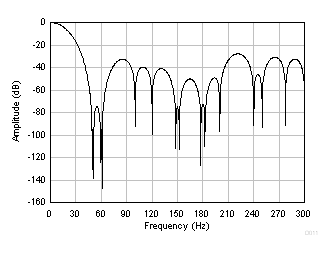
ADS125H02 D011_sbas661.gifFigure 74. FIR Frequency Response (20 SPS)
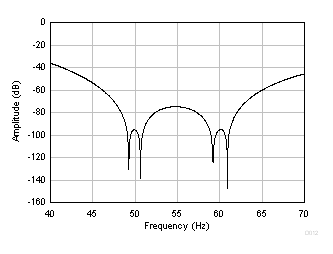
ADS125H02 D012_sbas661.gifFigure 75. FIR Frequency Response Detail (20 SPS)

Figure 76 shows the FIR filter response at 10 SPS. New frequency nulls are superimposed to the nulls in Figure 74 as a result of the variable averager. The first of the combined response nulls occurs at 10 Hz. Additional nulls occur at folded frequencies around multiples of 20 Hz. The first of the 10 SPS folded null frequencies is shown in Figure 76 at 10 Hz, 30 Hz, 70 Hz, 90 Hz, and so on.
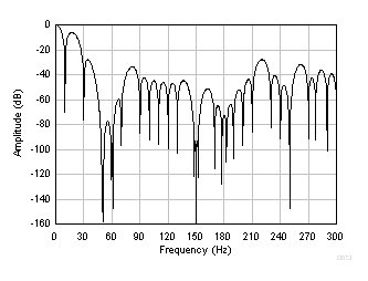
ADS125H02 D013_sbas661.gifFigure 76. FIR Frequency Response (10 SPS)

Similar to the response of the sinc filter, the overall FIR filter frequency has a low-pass response that rolls off high frequencies. The response is such that the FIR filter limits the bandwidth of the input signal. The signal bandwidth depends on the output data rate. Table 6 lists the –3-dB filter bandwidth of the FIR filter. The total system bandwidth is the combined response of the digital filter, the PGA antialias filter, and external filters.

Table 6. FIR Filter Bandwidth

DATA RATE (SPS) –3-dB BANDWIDTH (Hz)
2.5 1.2
5 2.4
10 4.7
20 13