JAJSF13C March   2018  – January 2019 ADS1260 , ADS1261

PRODUCTION DATA.  

  1. 特長
  2. アプリケーション
  3. 概要
    1.     Device Images
      1.      ブロック図
  4. 改訂履歴
  5. 概要(続き)
  6. Device Comparison Table
  7. Pin Configuration and Functions
    1.     Pin Functions
  8. Specifications
    1. 8.1 Absolute Maximum Ratings
    2. 8.2 ESD Ratings
    3. 8.3 Recommended Operating Conditions
    4. 8.4 Thermal Information
    5. 8.5 Electrical Characteristics
    6. 8.6 Timing Requirements
    7. 8.7 Switching Characteristics
    8. 8.8 Typical Characteristics
  9. Parameter Measurement Information
    1. 9.1 Noise Performance
  10. 10Detailed Description
    1. 10.1 Overview
    2. 10.2 Functional Block Diagram
    3. 10.3 Feature Description
      1. 10.3.1  Analog Inputs
        1. 10.3.1.1 ESD Diodes
        2. 10.3.1.2 Input Multiplexer
        3. 10.3.1.3 Temperature Sensor
        4. 10.3.1.4 Power-Supply Readback
        5. 10.3.1.5 Inputs Open
        6. 10.3.1.6 Internal VCOM Connection
        7. 10.3.1.7 Alternate Functions
      2. 10.3.2  PGA
        1. 10.3.2.1 PGA Bypass Mode
        2. 10.3.2.2 PGA Voltage Monitor
      3. 10.3.3  Reference Voltage
        1. 10.3.3.1 Internal Reference
        2. 10.3.3.2 External Reference
        3. 10.3.3.3 AVDD - AVSS Reference (Default)
        4. 10.3.3.4 Reference Monitor
      4. 10.3.4  Level-Shift Voltage (VBIAS)
      5. 10.3.5  Burn-Out Current Sources
      6. 10.3.6  Sensor-Excitation Current Sources (IDAC1 and IDAC2)
      7. 10.3.7  General-Purpose Input/Outputs (GPIOs)
      8. 10.3.8  Oversampling
      9. 10.3.9  Modulator
      10. 10.3.10 Digital Filter
        1. 10.3.10.1 Sinc Filter
          1. 10.3.10.1.1 Sinc Filter Frequency Response
        2. 10.3.10.2 FIR Filter
          1. 10.3.10.2.1 FIR Filter Frequency Response
        3. 10.3.10.3 Filter Bandwidth
        4. 10.3.10.4 50-Hz and 60-Hz Normal Mode Rejection
    4. 10.4 Device Functional Modes
      1. 10.4.1 Conversion Control
        1. 10.4.1.1 Continuous-Conversion Mode
        2. 10.4.1.2 Pulse-Conversion Mode
        3. 10.4.1.3 Conversion Latency
        4. 10.4.1.4 Start-Conversion Delay
      2. 10.4.2 Chop Mode
      3. 10.4.3 AC-Excitation Mode
      4. 10.4.4 ADC Clock Mode
      5. 10.4.5 Power-Down Mode
        1. 10.4.5.1 Hardware Power-Down
        2. 10.4.5.2 Software Power-Down
      6. 10.4.6 Reset
        1. 10.4.6.1 Power-on Reset
        2. 10.4.6.2 Reset by Pin
        3. 10.4.6.3 Reset by Command
      7. 10.4.7 Calibration
        1. 10.4.7.1 Offset and Full-Scale Calibration
          1. 10.4.7.1.1 Offset Calibration Registers
          2. 10.4.7.1.2 Full-Scale Calibration Registers
        2. 10.4.7.2 Offset Self-Calibration (SFOCAL)
        3. 10.4.7.3 Offset System-Calibration (SYOCAL)
        4. 10.4.7.4 Full-Scale Calibration (GANCAL)
        5. 10.4.7.5 Calibration Command Procedure
        6. 10.4.7.6 User Calibration Procedure
    5. 10.5 Programming
      1. 10.5.1 Serial Interface
        1. 10.5.1.1 Chip Select (CS)
        2. 10.5.1.2 Serial Clock (SCLK)
        3. 10.5.1.3 Data Input (DIN)
        4. 10.5.1.4 Data Output/Data Ready (DOUT/DRDY)
        5. 10.5.1.5 Serial Interface Auto-Reset
      2. 10.5.2 Data Ready (DRDY)
        1. 10.5.2.1 DRDY in Continuous-Conversion Mode
        2. 10.5.2.2 DRDY in Pulse-Conversion Mode
        3. 10.5.2.3 Data Ready by Software Polling
      3. 10.5.3 Conversion Data
        1. 10.5.3.1 Status byte (STATUS)
        2. 10.5.3.2 Conversion Data Format
      4. 10.5.4 CRC
      5. 10.5.5 Commands
        1. 10.5.5.1  NOP Command
        2. 10.5.5.2  RESET Command
        3. 10.5.5.3  START Command
        4. 10.5.5.4  STOP Command
        5. 10.5.5.5  RDATA Command
        6. 10.5.5.6  SYOCAL Command
        7. 10.5.5.7  GANCAL Command
        8. 10.5.5.8  SFOCAL Command
        9. 10.5.5.9  RREG Command
        10. 10.5.5.10 WREG Command
        11. 10.5.5.11 LOCK Command
        12. 10.5.5.12 UNLOCK Command
    6. 10.6 Register Map
      1. 10.6.1  Device Identification (ID) Register (address = 00h) [reset = xxh]
        1. Table 30. ID Register Field Descriptions
      2. 10.6.2  Device Status (STATUS) Register (address = 01h) [reset = 01h]
        1. Table 31. STATUS Register Field Descriptions
      3. 10.6.3  Mode 0 (MODE0) Register (address = 02h) [reset = 24h]
        1. Table 32. MODE0 Register Field Descriptions
      4. 10.6.4  Mode 1 (MODE1) Register (address = 03h) [reset = 01h]
        1. Table 33. MODE1 Register Field Descriptions
      5. 10.6.5  Mode 2 (MODE2) Register (address = 04h) [reset = 00h]
        1. Table 34. MODE2 Register Field Descriptions
      6. 10.6.6  Mode 3 (MODE3) Register (address = 05h) [reset = 00h]
        1. Table 35. MODE3 Register Field Descriptions
      7. 10.6.7  Reference Configuration (REF) Register (address = 06h) [reset = 05h]
        1. Table 36. REF Register Field Descriptions
      8. 10.6.8  Offset Calibration (OFCALx) Registers (address = 07h, 08h, 09h) [reset = 00h, 00h, 00h]
        1. Table 37. OFCAL0, OFCAL1, OFCAL2 Registers Field Description
      9. 10.6.9  Full-Scale Calibration (FSCALx) Registers (address = 0Ah, 0Bh, 0Ch) [reset = 00h, 00h, 40h]
        1. Table 38. FSCAL0, FSCAL1, FSCAL2 Registers Field Description
      10. 10.6.10 IDAC Multiplexer (IMUX) Register (address = 0Dh) [reset = FFh]
        1. Table 39. IMUX Register Field Descriptions
      11. 10.6.11 IDAC Magnitude (IMAG) Register (address = 0Eh) [reset = 00h]
        1. Table 40. IMAG Register Field Descriptions
      12. 10.6.12 Reserved (RESERVED) Register (address = 0Fh) [reset = 00h]
        1. Table 41. RESERVED Register Field Descriptions
      13. 10.6.13 PGA Configuration (PGA) Register (address = 10h) [reset = 00h]
        1. Table 42. PGA Register Field Descriptions
      14. 10.6.14 Input Multiplexer (INPMUX) Register (address = 11h) [reset = FFh]
        1. Table 43. INPMUX Register Field Descriptions
      15. 10.6.15 Input Bias (INPBIAS) Register (address = 12h) [reset = 00h]
        1. Table 44. INPBIAS Register Field Descriptions
  11. 11Application and Implementation
    1. 11.1 Application Information
      1. 11.1.1 Input Range
      2. 11.1.2 Input Overload
      3. 11.1.3 Burn-Out Current Source
      4. 11.1.4 Unused Inputs and Outputs
      5. 11.1.5 AC-Excitation
      6. 11.1.6 Serial Interface and Digital Connections
    2. 11.2 Typical Application
      1. 11.2.1 Design Requirements
      2. 11.2.2 Detailed Design Procedure
      3. 11.2.3 Application Curves
    3. 11.3 Initialization Setup
  12. 12Power Supply Recommendations
    1. 12.1 Power-Supply Decoupling
    2. 12.2 Analog Power-Supply Clamp
    3. 12.3 Power-Supply Sequencing
  13. 13Layout
    1. 13.1 Layout Guidelines
    2. 13.2 Layout Example
  14. 14デバイスおよびドキュメントのサポート
    1. 14.1 ドキュメントのサポート
      1. 14.1.1 関連資料
    2. 14.2 関連リンク
    3. 14.3 ドキュメントの更新通知を受け取る方法
    4. 14.4 コミュニティ・リソース
    5. 14.5 商標
    6. 14.6 静電気放電に関する注意事項
    7. 14.7 Glossary
  15. 15メカニカル、パッケージ、および注文情報

パッケージ・オプション

デバイスごとのパッケージ図は、PDF版データシートをご参照ください。

メカニカル・データ(パッケージ|ピン)
  • RHB|32
サーマルパッド・メカニカル・データ
発注情報

Switching Characteristics

over operating ambient temperature range, DVDD = 2.7 V to 5.25 V, and DOUT/DRDY load: 20 pF || 100 kΩ to DGND (unless otherwise noted); see Figure 8
PARAMETER MIN TYP MAX UNIT
SERIAL INTERFACE
tw(DRH) Pulse duration, DRDY high 16 1/fCLK
tp(CSDO) Propagation delay time, CS falling edge to DOUT/DRDY driven 0 50 ns
tp(SCDO1) Propagation delay time, SCLK rising edge to valid DOUT/DRDY 40 ns
th(SCDO1) Hold time, SCLK rising edge to invalid data on DOUT/DRDY 0 ns
th(SCDO2) Hold time, last SCLK falling edge of operation to invalid data on DOUT/DRDY 15 ns
tp(SCDO2) Propagation delay time, last SCLK falling edge to valid data ready function on DOUT/DRDY 110 ns
tp(CSDOZ) Propagation delay time, CS rising edge to DOUT/DRDY high impedance 50 ns
RESET
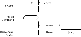
tp(RSCN) Propagation delay time, RESET rising edge or RESET command to start of conversion 512 1/fCLK
tp(PRCM) Propagation delay time, power-on threshold voltage to ADC communication 216 1/fCLK
tp(CMCN) Propagation delay time, ADC communication to conversion start 512 1/fCLK
AC EXCITATION
td(ACX) Delay time, phase-to-phase blanking period 8 1/fCLK
tc(ACX) ACX period 2 tSTDR
CONVERSION CONTROL
tp(STDR) Propagation delay time, START high or START command to DRDY high 2 1/fCLK
ADS1260 ADS1261 ai_tim_req_sbas760.gifFigure 1. Serial Interface Timing Requirements
ADS1260 ADS1261 ai_tim_char_sbas760.gifFigure 2. Serial Interface Switching Characteristics
ADS1260 ADS1261 ai_ser_auto_rst_sbas760.gifFigure 3. Serial Interface Auto-Reset Characteristics
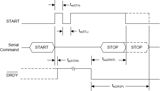
ADS1260 ADS1261 ai_start_stop_sbas760.gifFigure 4. Conversion Control Timing Requirements
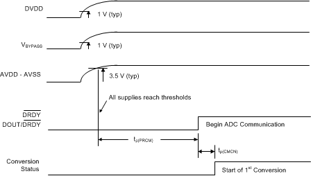
ADS1260 ADS1261 ai_por_sbas760.gifFigure 5. Power-Up Characteristics
ADS1260 ADS1261 ai_rst_timing_sbas760.gifFigure 6. RESET pin and RESET Command Timing Requirements
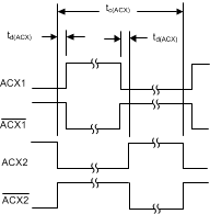
ADS1260 ADS1261 ai_acx_timing_sbas760.gifFigure 7. AC-Excitation Timing Characteristics
ADS1260 ADS1261 ai_tim_def_sbas760.gifFigure 8. Timing Voltage-Level Reference