JAJSIU8B June 2015 – April 2020 ADS131E08S
PRODUCTION DATA.
- 1 特長
- 2 アプリケーション
- 3 説明
- 4 改訂履歴
- 5 Device Comparison
- 6 Pin Configuration and Functions
- 7 Specifications
- 8 Parameter Measurement Information
-
9 Detailed Description
- 9.1 Overview
- 9.2 Functional Block Diagram
- 9.3 Feature Description
- 9.4 Device Functional Modes
- 9.5
Programming
- 9.5.1 SPI Interface
- 9.5.2 Data Retrieval
- 9.5.3
SPI Command Definitions
- 9.5.3.1 WAKEUP: Exit STANDBY Mode
- 9.5.3.2 STANDBY: Enter STANDBY Mode
- 9.5.3.3 RESET: Reset Registers to Default Values
- 9.5.3.4 START: Start Conversions
- 9.5.3.5 STOP: Stop Conversions
- 9.5.3.6 OFFSETCAL: Channel Offset Calibration
- 9.5.3.7 RDATAC: Start Read Data Continuous Mode
- 9.5.3.8 SDATAC: Stop Read Data Continuous Mode
- 9.5.3.9 RDATA: Read Data
- 9.5.3.10 RREG: Read from Register
- 9.5.3.11 WREG: Write to Register
- 9.5.3.12 Sending Multibyte Commands
- 9.6
Register Map
- 9.6.1
Register Descriptions
- 9.6.1.1 ID: ID Control Register (Factory-Programmed, Read-Only) (address = 00h) [reset = D2h]
- 9.6.1.2 CONFIG1: Configuration Register 1 (address = 01h) [reset = 94h]
- 9.6.1.3 CONFIG2: Configuration Register 2 (address = 02h) [reset = 00h]
- 9.6.1.4 CONFIG3: Configuration Register 3 (address = 03h) [reset = E0h]
- 9.6.1.5 FAULT: Fault Detect Control Register (address = 04h) [reset = 00h]
- 9.6.1.6 CHnSET: Individual Channel Settings (address = 05h to 0Ch) [reset = 10h]
- 9.6.1.7 FAULT_STATP: Fault Detect Positive Input Status (address = 12h) [reset = 00h]
- 9.6.1.8 FAULT_STATN: Fault Detect Negative Input Status (address = 13h) [reset = 00h]
- 9.6.1.9 GPIO: General-Purpose IO Register (address = 14h) [reset = 0Fh]
- 9.6.1
Register Descriptions
- 10Application and Implementation
- 11Power Supply Recommendations
- 12Layout
- 13デバイスおよびドキュメントのサポート
- 14メカニカル、パッケージ、および注文情報
9.3.7 Digital Decimation Filter
The digital filter receives the modulator output bit stream and decimates the data stream. The decimation ratio determines the number of samples taken to create the output data word, and is set by the modulator rate divided by the data rate (fMOD / fDR). By adjusting the decimation ratio, a tradeoff can be made between resolution and data rate: higher decimation allows for higher resolution (thus creating lower data rates) and lower decimation decreases resolution but enables wider bandwidths with higher data rates. Higher data rates are typically used in power applications that implement software re-sampling techniques to help with channel-to-channel phase adjustment for voltage and current.
The digital filter on each channel consists of a third-order sinc filter. An input step change takes three conversion cycles for the filter to settle. Adjust the decimation ratio of the sinc3 filters using the DR[2:0] bits in the CONFIG1 register (see the Register Map section for details). The data rate setting is a global setting that sets all channels to the same data rate.
The sinc filter is a variable decimation rate, third-order, low-pass filter. Data are supplied to this section of the filter from the modulator at the rate of fMOD. The sinc3 filter attenuates the high-frequency modulator noise, then decimates the data stream into parallel data. The decimation rate affects the overall converter data rate.
Equation 5 shows the scaled sinc3 filter Z-domain transfer function.

The sinc3 filter frequency domain transfer function is shown in Equation 6.
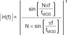
where
- N = decimation ratio
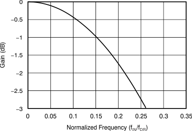
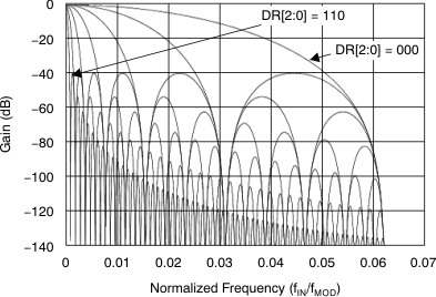
The sinc3 filter has notches (or zeroes) that occur at the output data rate and multiples thereof. At these frequencies, the filter has infinite attenuation. Figure 24 illustrates the sinc filter frequency response and Figure 25 illustrates the sinc filter roll-off. Figure 26 and Figure 27 illustrate the filter transfer function until fMOD / 2 and fMOD / 16, respectively, at different data rates. Figure 28 illustrates the transfer function extended until 4 fMOD. Figure 28 illustrates that the ADS131E08S passband repeats itself at every fMOD. Note that the digital filter response and filter notches are proportional to the master clock frequency.
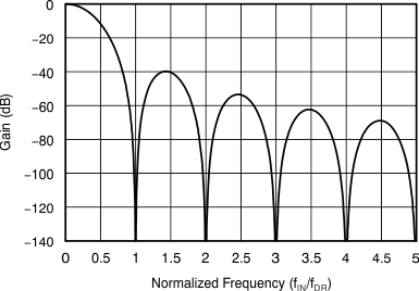
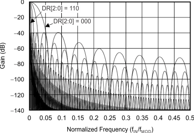
![ADS131E08S Transfer Function of Decimation Filters Until 4 fMOD for DR[2:0] = 000 and DR[2:0] = 110 ADS131E08S ai_tx_funct_bas561.gif](/ods/images/JAJSIU8B/ai_tx_funct_bas561.gif)
Until 4 fMOD for DR[2:0] = 000 and DR[2:0] = 110
