SLAS900F October   2012  – December 2014 ADS42JB49 , ADS42JB69

PRODUCTION DATA.  

  1. Features
  2. Applications
  3. Description
  4. Revision History
  5. Device Comparison Table
  6. Pin Configuration and Functions
  7. Specifications
    1. 7.1  Absolute Maximum Ratings
    2. 7.2  ESD Ratings
    3. 7.3  Recommended Operating Conditions
    4. 7.4  Thermal Information
    5. 7.5  Electrical Characteristics: ADS42JB69 (16-Bit)
    6. 7.6  Electrical Characteristics: ADS42JB49 (14-Bit)
    7. 7.7  Electrical Characteristics: General
    8. 7.8  Digital Characteristics
    9. 7.9  Timing Characteristics
    10. 7.10 Typical Characteristics: ADS42JB69
    11. 7.11 Typical Characteristics: ADS42JB49
    12. 7.12 Typical Characteristics: Common
    13. 7.13 Typical Characteristics: Contour
      1. 7.13.1 Spurious-Free Dynamic Range (SFDR): General
      2. 7.13.2 Signal-to-Noise Ratio (SNR): ADS42JB69
      3. 7.13.3 Signal-to-Noise Ratio (SNR): ADS42JB49
  8. Parameter Measurement Information
  9. Detailed Description
    1. 9.1 Overview
    2. 9.2 Functional Block Diagram
    3. 9.3 Feature Description
      1. 9.3.1 Digital Gain
      2. 9.3.2 Input Clock Divider
      3. 9.3.3 Overrange Indication
      4. 9.3.4 Pin Controls
    4. 9.4 Device Functional Modes
      1. 9.4.1 JESD204B Interface
        1. 9.4.1.1 JESD204B Initial Lane Alignment (ILA)
        2. 9.4.1.2 JESD204B Test Patterns
        3. 9.4.1.3 JESD204B Frame Assembly
        4. 9.4.1.4 JESD Link Configuration
          1. 9.4.1.4.1 Configuration for 2-Lane (20x) SERDES Mode
          2. 9.4.1.4.2 Configuration for 4-Lane (10x) SERDES Mode
        5. 9.4.1.5 CML Outputs
    5. 9.5 Programming
      1. 9.5.1 Device Configuration
      2. 9.5.2 Details of Serial Interface
        1. 9.5.2.1 Register Initialization
        2. 9.5.2.2 Serial Register Write
        3. 9.5.2.3 Serial Register Readout
    6. 9.6 Register Maps
      1. 9.6.1 Description of Serial Interface Registers
        1. 9.6.1.1  Register 6 (offset = 06h) [reset = 00h]
        2. 9.6.1.2  Register 7 (offset = 07h) [reset = 00h]
        3. 9.6.1.3  Register 8 (offset = 08h) [reset = 00h]
        4. 9.6.1.4  Register B (offset = 0Bh) [reset = 00h]
        5. 9.6.1.5  Register C (offset = 0Ch) [reset = 00h]
        6. 9.6.1.6  Register D (offset = 0Dh) [reset = 00h]
        7. 9.6.1.7  Register E (offset = 0Eh) [reset = 00h]
        8. 9.6.1.8  Register F (offset = 0Fh) [reset = 00h]
        9. 9.6.1.9  Register 10 (offset = 10h) [reset = 00h]
        10. 9.6.1.10 Register 11 (offset = 11h) [reset = 00h]
        11. 9.6.1.11 Register 12 (offset = 12h) [reset = 00h]
        12. 9.6.1.12 Register 13 (offset = 13h) [reset = 00h]
        13. 9.6.1.13 Register 1F (offset = 1Fh) [reset = FFh]
        14. 9.6.1.14 Register 26 (offset = 26h) [reset = 00h]
        15. 9.6.1.15 Register 27 (offset = 27h) [reset = 00h]
        16. 9.6.1.16 Register 2B (offset = 2Bh) [reset = 00h]
        17. 9.6.1.17 Register 2C (offset = 2Ch) [reset = 00h]
        18. 9.6.1.18 Register 2D (offset = 2Dh) [reset = 00h]
        19. 9.6.1.19 Register 30 (offset = 30h) [reset = 40h]
        20. 9.6.1.20 Register 36 (offset = 36h) [reset = 00h]
        21. 9.6.1.21 Register 37 (offset = 37h) [reset = 00h]
        22. 9.6.1.22 Register 38 (offset = 38h) [reset = 00h]
  10. 10Application and Implementation
    1. 10.1 Application Information
    2. 10.2 Typical Application
      1. 10.2.1 Design Requirements
      2. 10.2.2 Detailed Design Procedure
        1. 10.2.2.1 Analog Input
          1. 10.2.2.1.1 Drive Circuit Requirements
          2. 10.2.2.1.2 Driving Circuit
        2. 10.2.2.2 Clock Input
          1. 10.2.2.2.1 SNR and Clock Jitter
      3. 10.2.3 Application Curves
  11. 11Power Supply Recommendations
  12. 12Layout
    1. 12.1 Layout Guidelines
    2. 12.2 Layout Example
  13. 13Device and Documentation Support
    1. 13.1 Device Support
      1. 13.1.1 Device Nomenclature
        1. 13.1.1.1 Definition of Specifications
    2. 13.2 Documentation Support
      1. 13.2.1 Related Documentation
    3. 13.3 Related Links
    4. 13.4 Trademarks
    5. 13.5 Electrostatic Discharge Caution
    6. 13.6 Glossary
  14. 14Mechanical, Packaging, and Orderable Information

パッケージ・オプション

メカニカル・データ(パッケージ|ピン)
サーマルパッド・メカニカル・データ
発注情報

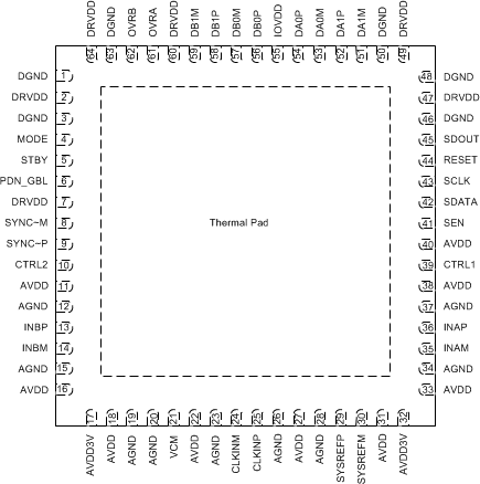
6 Pin Configuration and Functions

RGC Package
VQFN-64
(Top View)
po2_las900.gif

Pin Functions: JESD204B Output Interface

PIN I/O FUNCTION DESCRIPTION
NAME NO.
AGND 12, 15, 19, 20, 23, 26, 28, 34, 37 I Supply Analog ground
AVDD 11, 16, 18, 22, 27, 31, 33, 38, 40 I Supply 1.8-V analog power supply
AVDD3V 17, 32 I Supply 3.3-V analog supply for analog buffer
CLKINM 24 I Clock Differential ADC clock input
CLKINP 25 I Clock Differential ADC clock input
CTRL1 39 I Control Power-down control with an internal 150-kΩ pull-down resistor
CTRL2 10 I Control Power-down control with an internal 150-kΩ pull-down resistor
DA0P/M 54, 53 O Interface JESD204B serial data output for channel A, lane 0
DA1P/M 52,51 O Interface JESD204B serial data output for channel A, lane 1
DB0P/M 56,57 O Interface JESD204B serial data output for channel B, lane 0
DB1P/M 58,59 O Interface JESD204B serial data output for channel B, lane 1
DGND 1, 3, 46, 48, 50, 63 I Supply Digital ground
DRVDD 2, 7, 47, 49, 60, 64 I Supply Digital 1.8-V power supply
INAM 35 I Input Differential analog input for channel A
INAP 36 I Input Differential analog input for channel A
INBM 14 I Input Differential analog input for channel B
INBP 13 I Input Differential analog input for channel B
IOVDD 55 I Supply Digital 1.8-V power supply for the JESD204B transmitter
MODE 4 I Control Connect to GND
OVRA 61 O Interface Overrange indication channel A in CMOS output format.
OVRB 62 O Interface Overrange indication channel B in CMOS output format.
PDN_GBL 6 I Control Global power down. Active high with an internal 150-kΩ pull-down resistor.
RESET 44 I Control Hardware reset; active high. This pin has an internal 150-kΩ pull-down resistor.
SCLK 43 I Control Serial interface clock input. This pin has an internal 150-kΩ pull-down resistor.
SDATA 42 I Control Serial interface data input. This pin has an internal 150-kΩ pull-down resistor.
SDOUT 45 O Control Serial interface data output
SEN 41 I Control Serial interface enable. This pin has an internal 150-kΩ pull-up resistor.
STBY 5 I Control Standby. Active high with an internal 150-kΩ pull-down resistor.
SYNC~P 9 I Interface Synchronization input for JESD204B port
SYNC~M 8 I Interface Synchronization input for JESD204B port
SYSREFM 30 I Clock External SYSREF input (subclass 1)
SYSREFP 29 I Clock External SYSREF input (subclass 1)
VCM 21 O Output 1.9-V common-mode output voltage for analog inputs
Thermal pad GND Ground Connect to ground plane