SLAS900F October 2012 – December 2014 ADS42JB49 , ADS42JB69
PRODUCTION DATA.
- 1 Features
- 2 Applications
- 3 Description
- 4 Revision History
- 5 Device Comparison Table
- 6 Pin Configuration and Functions
-
7 Specifications
- 7.1 Absolute Maximum Ratings
- 7.2 ESD Ratings
- 7.3 Recommended Operating Conditions
- 7.4 Thermal Information
- 7.5 Electrical Characteristics: ADS42JB69 (16-Bit)
- 7.6 Electrical Characteristics: ADS42JB49 (14-Bit)
- 7.7 Electrical Characteristics: General
- 7.8 Digital Characteristics
- 7.9 Timing Characteristics
- 7.10 Typical Characteristics: ADS42JB69
- 7.11 Typical Characteristics: ADS42JB49
- 7.12 Typical Characteristics: Common
- 7.13 Typical Characteristics: Contour
- 8 Parameter Measurement Information
-
9 Detailed Description
- 9.1 Overview
- 9.2 Functional Block Diagram
- 9.3 Feature Description
- 9.4 Device Functional Modes
- 9.5 Programming
- 9.6
Register Maps
- 9.6.1
Description of Serial Interface Registers
- 9.6.1.1 Register 6 (offset = 06h) [reset = 00h]
- 9.6.1.2 Register 7 (offset = 07h) [reset = 00h]
- 9.6.1.3 Register 8 (offset = 08h) [reset = 00h]
- 9.6.1.4 Register B (offset = 0Bh) [reset = 00h]
- 9.6.1.5 Register C (offset = 0Ch) [reset = 00h]
- 9.6.1.6 Register D (offset = 0Dh) [reset = 00h]
- 9.6.1.7 Register E (offset = 0Eh) [reset = 00h]
- 9.6.1.8 Register F (offset = 0Fh) [reset = 00h]
- 9.6.1.9 Register 10 (offset = 10h) [reset = 00h]
- 9.6.1.10 Register 11 (offset = 11h) [reset = 00h]
- 9.6.1.11 Register 12 (offset = 12h) [reset = 00h]
- 9.6.1.12 Register 13 (offset = 13h) [reset = 00h]
- 9.6.1.13 Register 1F (offset = 1Fh) [reset = FFh]
- 9.6.1.14 Register 26 (offset = 26h) [reset = 00h]
- 9.6.1.15 Register 27 (offset = 27h) [reset = 00h]
- 9.6.1.16 Register 2B (offset = 2Bh) [reset = 00h]
- 9.6.1.17 Register 2C (offset = 2Ch) [reset = 00h]
- 9.6.1.18 Register 2D (offset = 2Dh) [reset = 00h]
- 9.6.1.19 Register 30 (offset = 30h) [reset = 40h]
- 9.6.1.20 Register 36 (offset = 36h) [reset = 00h]
- 9.6.1.21 Register 37 (offset = 37h) [reset = 00h]
- 9.6.1.22 Register 38 (offset = 38h) [reset = 00h]
- 9.6.1
Description of Serial Interface Registers
- 10Application and Implementation
- 11Power Supply Recommendations
- 12Layout
- 13Device and Documentation Support
- 14Mechanical, Packaging, and Orderable Information
7 Specifications
7.1 Absolute Maximum Ratings
over operating free-air temperature range (unless otherwise noted)(1)| MIN | MAX | UNIT | ||
|---|---|---|---|---|
| Supply voltage | AVDD3V | –0.3 | 3.6 | V |
| AVDD | –0.3 | 2.1 | V | |
| DRVDD | –0.3 | 2.1 | V | |
| IOVDD | –0.3 | 2.1 | V | |
| Voltage between AGND and DGND | –0.3 | 0.3 | V | |
| Voltage applied to input pins | INAP, INBP, INAM, INBM | –0.3 | 3 | V |
| CLKINP, CLKINM | –0.3 | minimum (2.1, AVDD + 0.3) | V | |
| SYNC~P, SYNC~M | –0.3 | minimum (2.1, AVDD + 0.3) | V | |
| SYSREFP, SYSREFM | –0.3 | minimum (2.1, AVDD + 0.3) | V | |
| SCLK, SEN, SDATA, RESET, PDN_GBL, CTRL1, CTRL2, STBY, MODE | –0.3 | 3.9 | V | |
| Temperature | Operating free-air, TA | –40 | +85 | °C |
| Operating junction, TJ | +125 | °C | ||
| Storage, Tstg | –65 | +150 | °C | |
(1) Stresses beyond those listed under Absolute Maximum Ratings may cause permanent damage to the device. These are stress ratings only, which do not imply functional operation of the device at these or any other conditions beyond those indicated under Recommended Operating Conditions. Exposure to absolute-maximum-rated conditions for extended periods may affect device reliability.
7.2 ESD Ratings
| VALUE | UNIT | |||
|---|---|---|---|---|
| V(ESD) | Electrostatic discharge | Human body model (HBM), per ANSI/ESDA/JEDEC JS-001(1) | ±2000 | V |
(1) JEDEC document JEP155 states that 500-V HBM allows safe manufacturing with a standard ESD control process.
7.3 Recommended Operating Conditions
over operating free-air temperature range (unless otherwise noted)(3)| MIN | NOM | MAX | UNIT | |||
|---|---|---|---|---|---|---|
| SUPPLIES | ||||||
| AVDD | Analog supply voltage | 1.7 | 1.8 | 1.9 | V | |
| AVDD3V | Analog buffer supply voltage | 3.15 | 3.3 | 3.45 | V | |
| DRVDD | Digital supply voltage | 1.7 | 1.8 | 1.9 | V | |
| IOVDD | Output buffer supply voltage | 1.7 | 1.8 | 1.9 | V | |
| ANALOG INPUTS | ||||||
| VID | Differential input voltage range | Default after reset | 2 | VPP | ||
| Register programmable(1) | 2.5 | VPP | ||||
| VICR | Input common-mode voltage | VCM ± 0.025 | V | |||
| Maximum analog input frequency with 2.5-VPP input amplitude | 250 | MHz | ||||
| Maximum analog input frequency with 2-VPP input amplitude | 400 | MHz | ||||
| CLOCK INPUT | ||||||
| Input clock sample rate | 10x mode | 60 | 250 | MSPS | ||
| 20x mode | 40 | 156.25 | MSPS | |||
| Input clock amplitude differential (VCLKP – VCLKM) |
Sine wave, ac-coupled | 0.3(2) | 1.5 | VPP | ||
| LVPECL, ac-coupled | 1.6 | VPP | ||||
| LVDS, ac-coupled | 0.7 | VPP | ||||
| LVCMOS, single-ended, ac-coupled | 1.5 | V | ||||
| Input clock duty cycle | 35% | 50% | 65% | |||
| DIGITAL OUTPUTS | ||||||
| CLOAD | Maximum external load capacitance from each output pin to DRGND | 3.3 | pF | |||
| RLOAD | Single-ended load resistance | +50 | Ω | |||
| TA | Operating free-air temperature | –40 | +85 | °C | ||
(1) For details, refer to the Digital Gain section.
(3) After power-up, to reset the device for the first time, use the RESET pin only. Refer to the Register Initialization section.
7.4 Thermal Information
| THERMAL METRIC(1) | ADS42JBx9 | UNIT | |
|---|---|---|---|
| RGC (QFN) | |||
| 64 PINS | |||
| RθJA | Junction-to-ambient thermal resistance | 22.9 | °C/W |
| RθJC(top) | Junction-to-case (top) thermal resistance | 7.1 | |
| RθJB | Junction-to-board thermal resistance | 2.5 | |
| ψJT | Junction-to-top characterization parameter | 0.1 | |
| ψJB | Junction-to-board characterization parameter | 2.5 | |
| RθJC(bot) | Junction-to-case (bottom) thermal resistance | 0.2 | |
(1) For more information about traditional and new thermal metrics, see the IC Package Thermal Metrics application report, SPRA953.
7.5 Electrical Characteristics: ADS42JB69 (16-Bit)
Typical values are at TA = +25°C, AVDD = 1.8 V, AVDD3V = 3.3 V, DRVDD = 1.8 V, IOVDD = 1.8 V, 50% clock duty cycle, –1-dBFS differential analog input, and sampling rate = 250 MSPS, unless otherwise noted. Minimum and maximum values are across the full temperature range of TMIN = –40°C to TMAX = +85°C, AVDD = 1.8 V, AVDD3V = 3.3 V, DRVDD = 1.8 V, and IOVDD = 1.8 V.7.6 Electrical Characteristics: ADS42JB49 (14-Bit)
Typical values are at TA = +25°C, AVDD = 1.8 V, AVDD3V = 3.3 V, DRVDD = 1.8 V, IOVDD = 1.8 V, 50% clock duty cycle, –1-dBFS differential analog input, and sampling rate = 250 MSPS, unless otherwise noted. Minimum and maximum values are across the full temperature range of TMIN = –40°C to TMAX = +85°C, AVDD = 1.8 V, AVDD3V = 3.3 V, DRVDD = 1.8 V, and IOVDD = 1.8 V.7.7 Electrical Characteristics: General
Typical values are at +25°C, AVDD = 1.8 V, AVDD3V = 3.3 V, DRVDD = 1.8 V, IOVDD = 1.8 V, 50% clock duty cycle, –1-dBFS differential analog input, and sampling rate = 250 MSPS, unless otherwise noted. Minimum and maximum values are across the full temperature range: TMIN = –40°C to TMAX = +85°C, AVDD = 1.8 V, AVDD3V = 3.3 V, DRVDD = 1.8 V, and IOVDD = 1.8 V.| PARAMETER | TEST CONDITIONS | MIN | TYP | MAX | UNIT | |
|---|---|---|---|---|---|---|
| ANALOG INPUTS | ||||||
| VID | Differential input voltage range | Default (after reset) | 2 | VPP | ||
| Register programmed(1) | 2.5 | VPP | ||||
| Differential input resistance (at 170 MHz) | 1.2 | kΩ | ||||
| Differential input capacitance (at 170 MHz) | 4 | pF | ||||
| Analog input bandwidth | With 50-Ω source impedance, and 50-Ω termination | 900 | MHz | |||
| VCM | Common-mode output voltage | 1.9 | V | |||
| VCM output current capability | 10 | mA | ||||
| DC ACCURACY | ||||||
| Offset error | –20 | 20 | mV | |||
| EGREF | Gain error as a result of internal reference inaccuracy alone | ±2 | %FS | |||
| EGCHAN | Gain error of channel alone | –5 | %FS | |||
| Temperature coefficient of EGCHAN | 0.01 | Δ%/°C | ||||
| POWER SUPPLY | ||||||
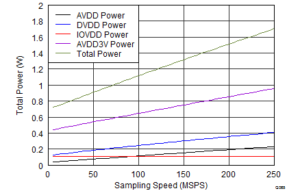
| IAVDD | Analog supply current | 128 | 160 | mA | ||
| IAVDD3V | Analog buffer supply current | 290 | 330 | mA | ||
| IDRVDD | Digital supply current | 228 | 252 | mA | ||
| IOVDD | Output buffer supply current | 50-Ω external termination from pin to IOVDD, fIN = 2.5 MHz | 60 | 100 | mA | |
| Analog power | 231 | mW | ||||
| Analog buffer power | 957 | mW | ||||
| Digital power | 410 | mW | ||||
| Power consumption by output buffer | 50-Ω external termination from pin to IOVDD, fIN = 2.5 MHz | 109 | mW | |||
| Total power | 1.7 | 1.96 | W | |||
| Global power-down | 160 | mW | ||||
(1) Refer to the Serial Interface section.
7.8 Digital Characteristics
The dc specifications refer to the condition where the digital outputs are not switching, but are permanently at a valid logic level '0' or '1'. AVDD = 1.8 V, AVDD3V = 3.3 V, DRVDD = 1.8 V, and IOVDD = 1.8 V, unless otherwise noted.| PARAMETER | TEST CONDITIONS | MIN | TYP | MAX | UNIT | |
|---|---|---|---|---|---|---|
| DIGITAL INPUTS (RESET, SCLK, SEN, SDATA, PDN_GBL, STBY, CTRL1, CTRL2, MODE)(1) | ||||||
| High-level input voltage | All digital inputs support 1.8-V and 3.3-V logic levels | 1.2 | V | |||
| Low-level input voltage | All digital inputs support 1.8-V and 3.3-V logic levels | 0.4 | V | |||
| High-level input current | SEN | 0 | µA | |||
| RESET, SCLK, SDATA, PDN_GBL, STBY, CTRL1, CTRL2, MODE | 10 | µA | ||||
| Low-level input current | SEN | 10 | µA | |||
| RESET, SCLK, SDATA, PDN_GBL, STBY, CTRL1, CTRL2, MODE | 0 | µA | ||||
| DIGITAL INPUTS (SYNC~P, SYNC~M, SYSREFP, SYSREFM) | ||||||
| High-level input voltage | 1.3 | V | ||||
| Low-level input voltage | 0.5 | V | ||||
| VCM_DIG | Input common-mode voltage | 0.9 | V | |||
| DIGITAL OUTPUTS (SDOUT, OVRA, OVRB) | ||||||
| High-level output voltage | DRVDD – 0.1 | DRVDD | V | |||
| Low-level output voltage | 0.1 | V | ||||
| DIGITAL OUTPUTS (JESD204B Interface: DA[0,1], DB[0,1])(2) | ||||||
| High-level output voltage | IOVDD | V | ||||
| Low-level output voltage | IOVDD – 0.4 | V | ||||
| |VOD| | Output differential voltage | 0.4 | V | |||
| VOCM | Output common-mode voltage | IOVDD – 0.2 | V | |||
| Transmitter short-circuit current | Transmitter terminals shorted to any voltage between –0.25 V and 1.45 V | –100 | 100 | mA | ||
| Single-ended output impedance | 50 | Ω | ||||
| Output capacitance | Output capacitance inside the device, from either output to ground |
2 | pF | |||
(1) RESET, SCLK, SDATA, PDN_GBL, STBY, CTRL1, CTRL2 and MODE pins have 150-kΩ (typical) internal pull-down resistor to ground, while SEN pin has 150-kΩ (typical) pull-up resistor to AVDD.
(2) 50-Ω, single-ended external termination to IOVDD.
7.9 Timing Characteristics
Typical values are at +25°C, AVDD = 1.8 V, AVDD3V = 3.3 V, DRVDD = 1.8 V, IOVDD = 1.8 V, 50% clock duty cycle, –1-dBFS differential analog input, and sampling rate = 250 MSPS, unless otherwise noted. Minimum and maximum values are across the full temperature range: TMIN = –40°C to TMAX = +85°C, AVDD = 1.8 V, AVDD3V = 3.3 V, DRVDD = 1.8 V, and IOVDD = 1.8 V. See Figure 1.| PARAMETER | TEST CONDITIONS | MIN | TYP | MAX | UNIT | |||
|---|---|---|---|---|---|---|---|---|
| SAMPLE TIMING CHARACTERISTICS | ||||||||
| Aperture delay | 0.4 | 0.7 | 1.1 | ns | ||||
| Aperture delay matching | Between two channels on the same device | ±70 | ps | |||||
| Between two devices at the same temperature and supply voltage | ±150 | ps | ||||||
| Aperture jitter | 85 | fS rms | ||||||
| Wake-up time | Time to valid data after coming out of STANDBY mode | 50 | 200 | µs | ||||
| Time to valid data after coming out of global power-down | 250 | 1000 | µs | |||||
| tSU_SYNC~ | Setup time for SYNC~ | Referenced to input clock rising edge | 400 | ps | ||||
| tH_SYNC~ | Hold time for SYNC~ | Referenced to input clock rising edge | 100 | ps | ||||
| tSU_SYSREF | Setup time for SYSREF | Referenced to input clock rising edge | 400 | ps | ||||
| tH_SYSREF | Hold time for SYSREF | Referenced to input clock rising edge | 100 | ps | ||||
| CML OUTPUT TIMING CHARACTERISTICS | ||||||||
| Unit interval | 320 | 1667 | ps | |||||
| Serial output data rate | 3.125 | Gbps | ||||||
| Total jitter | 2.5 Gbps (10x mode, fS = 250 MSPS) | 0.28 | P-PUI | |||||
| 3.125 Gbps (20x mode, fS = 156.25 MSPS) | 0.3 | P-PUI | ||||||
| tR, tF | Data rise time, data fall time |
Rise and fall times measured from 20% to 80%, differential output waveform, 600 Mbps ≤ bit rate ≤ 3.125 Gbps |
105 | ps | ||||
Table 1. Latency in Different Modes(1)(2)
| MODE | PARAMETER | LATENCY (N Cycles) | TYPICAL DATA DELAY (tD, ns) |
|---|---|---|---|
| 10x | ADC latency | 23 | 0.65 × tS + 3 |
| Normal OVR latency | 14 | 6.7 | |
| Fast OVR latency | 9 | 6.7 | |
| from SYNC~ falling edge to CGS phase(3) | 16 | 0.65 × tS + 3 | |
| from SYNC~ rising edge to ILA sequence(4) | 25 | 0.65 × tS + 3 | |
| 20x | ADC latency | 22 | 0.85 × tS + 3 |
| Normal OVR latency | 14 | 6.7 | |
| Fast OVR latency | 9 | 6.7 | |
| from SYNC~ falling edge to CGS phase(3) | 15 | 0.85 × tS + 3 | |
| from SYNC~ rising edge to ILA sequence(4) | 16 | 0.85 × tS + 3 |
(1) Overall latency = latency + tD.
(2) tS is the time period of the ADC conversion clock.
(3) Latency is specified for subclass 2. In subclass 0, the SYNC~ falling edge to CGS phase latency is 16 clock cycles in 10x mode and 15 clock cycles in 20x mode.
(4) Latency is specified for subclass 2. In subclass 0, the SYNC~ rising edge to ILA sequence latency is 11 clock cycles in 10x mode and 11 clock cycles in 20x mode.
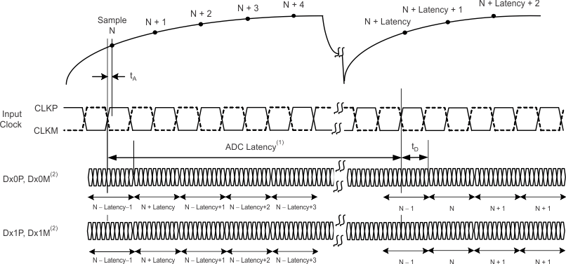
1. Overall latency = ADC latency + tD.
2. x = A for channel A and B for channel B.
Figure 1. ADC Latency
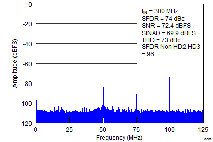
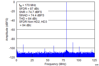
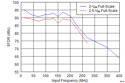
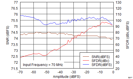
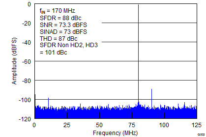
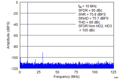
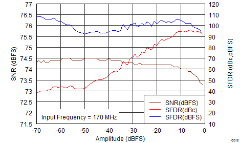
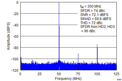
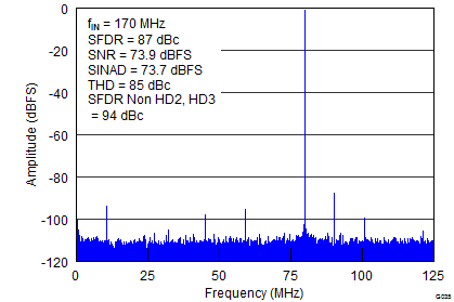
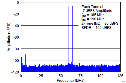
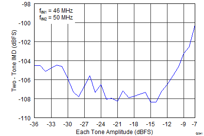
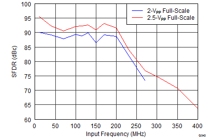
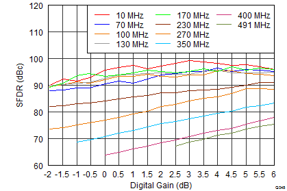
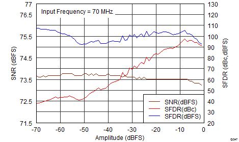
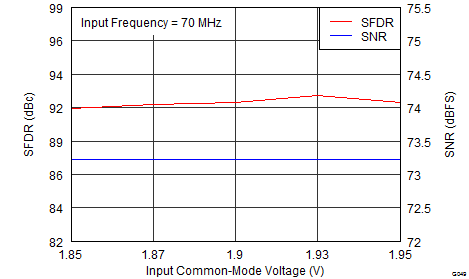
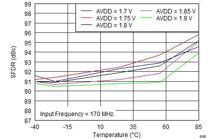
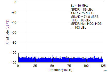
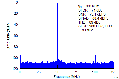
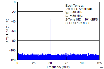
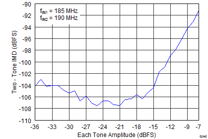
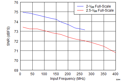
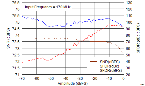
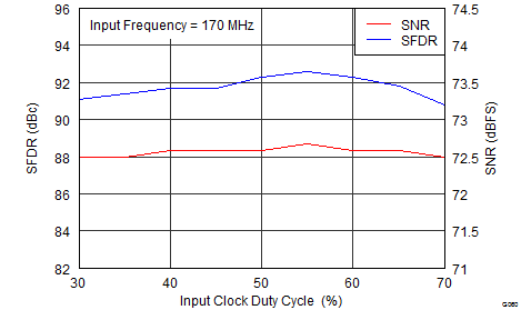
7.10 Typical Characteristics: ADS42JB69
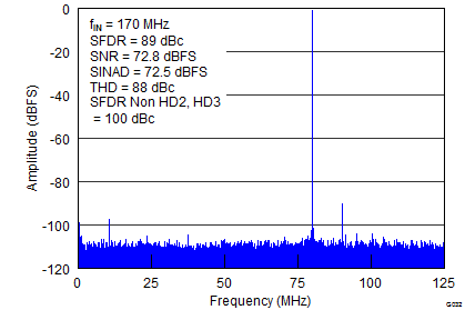
Typical values are at TA = +25°C, ADC sampling rate = 250 MSPS, 50% clock duty cycle, AVDD = 1.8 V, AVDD3V = 3.3 V, DRVDD = 1.8 V, IOVDD = 1.8 V, –1-dBFS differential input, 2-VPP full-scale, and 32k-point FFT, unless otherwise noted.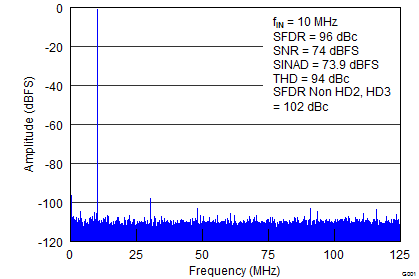
(2.5-VPP Full-Scale)
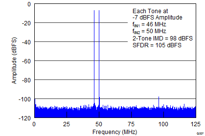
(–7 dBFS at 46 MHz and 50 MHz)

(–7 dBFS at 185 MHz and 190 MHz)
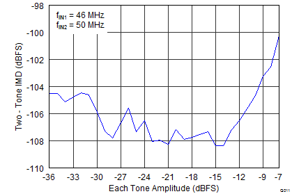
Input Amplitude (46 MHz and 50 MHz)
Input Frequency
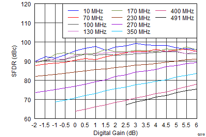
Digital Gain
(70 MHz)
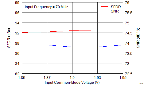
Input Common-Mode Voltage (70 MHz)
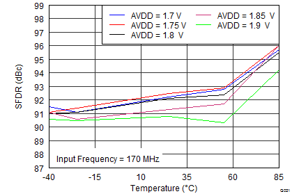
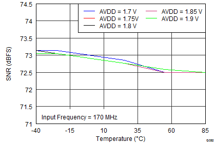
AVDD Supply and Temperature (170 MHz)
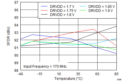
DRVDD Supply and Temperature (170 MHz)
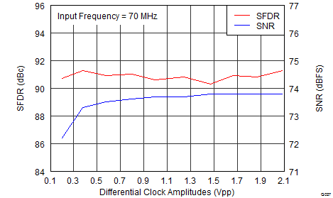
(70 MHz)
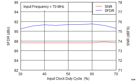
(70 MHz)
(2.5-VPP Full-Scale)

(2.5-VPP Full-Scale)

(–36 dBFS at 46 MHz and 50 MHz)
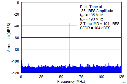
(–36 dBFS at 185 MHz and 190 MHz)

Input Amplitude (185 MHz and 190 MHz)
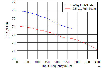
Input Frequency
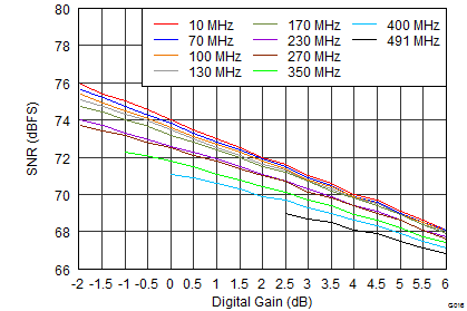
Digital Gain
(170 MHz)
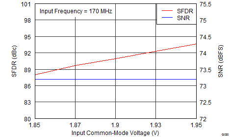
Input Common-Mode Voltage (170 MHz)
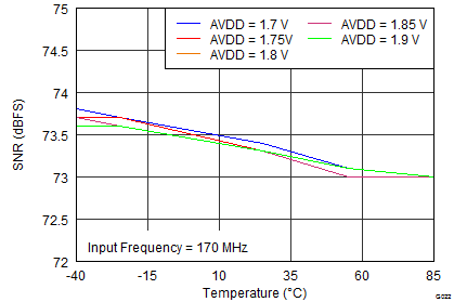
AVDD Supply and Temperature (170 MHz)
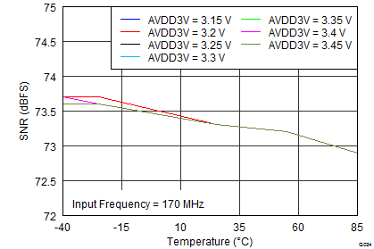
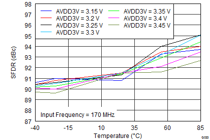
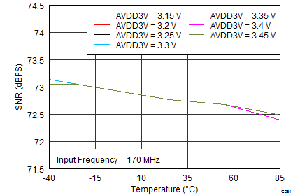
AVDD_BUF Supply and Temperature (170 MHz)
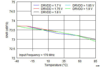
DRVDD Supply and Temperature (170 MHz)
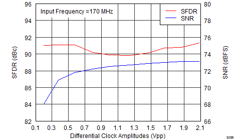
(170 MHz)
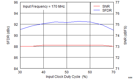
(170 MHz)
7.11 Typical Characteristics: ADS42JB49
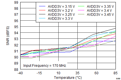
Typical values are at TA = +25°C, full temperature range is TMIN = –40°C to TMAX = +85°C, ADC sampling rate = 250 MSPS, 50% clock duty cycle, AVDD = 1.8 V, AVDD3V = 3.3 V, DRVDD = 1.8 V, IOVDD = 1.8 V, –1-dBFS differential input, 2-VPP full-scale, and 32k-point FFT, unless otherwise noted.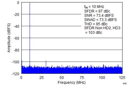
(2.5-VPP Full-Scale)

(–7 dBFS at 46 MHz and 50 MHz)
(–7 dBFS at 185 MHz and 190 MHz)
Input Amplitude (46 MHz and 50 MHz)
Input Frequency
Digital Gain
(70 MHz)
Input Common-Mode Voltage (70 MHz)
AVDD Supply and Temperature (170 MHz)
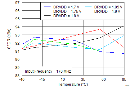
DRVDD Supply and Temperature (170 MHz)
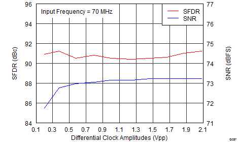
(70 MHz)
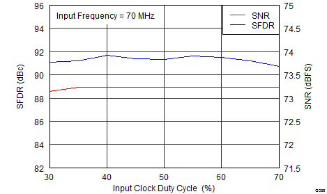
(70 MHz)
(2.5-VPP Full-Scale)
(2.5-VPP Full-Scale)
(–36 dBFS at 46 MHz and 50 MHz)

(–36 dBFS at 185 MHz and 190 MHz)
Input Amplitude (185 MHz and 190 MHz)
Input Frequency
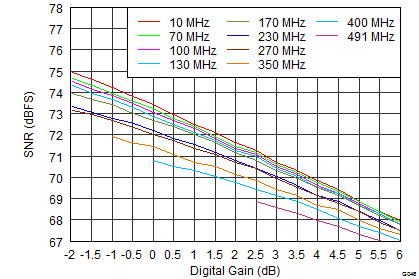
Digital Gain
(170 MHz)
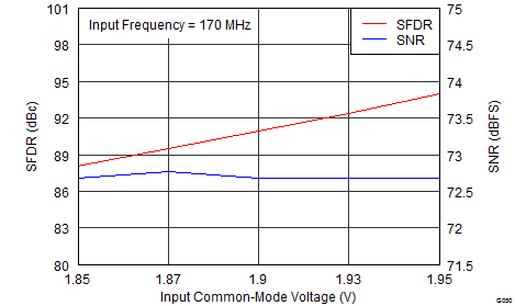
Input Common-Mode Voltage (170 MHz)
AVDD Supply and Temperature (170 MHz)
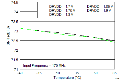
DRVDD Supply and Temperature (170 MHz)
(170 MHz)
(170 MHz)
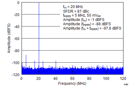
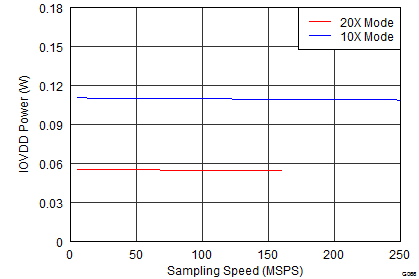
7.12 Typical Characteristics: Common
Typical values are at TA = +25°C, full temperature range is TMIN = –40°C to TMAX = +85°C, ADC sampling rate = 250 MSPS, 50% clock duty cycle, AVDD = 1.8 V, AVDD3V = 3.3 V, DRVDD = 1.8 V, IOVDD = 1.8 V, –1-dBFS differential input, 2-VPP full-scale, and 64k-point FFT, unless otherwise noted.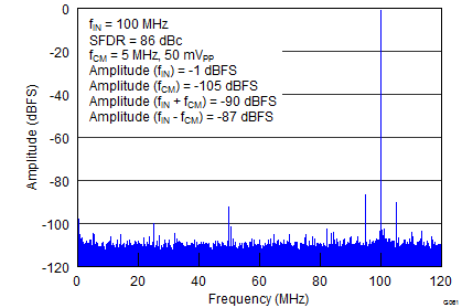
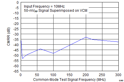
Test Signal Frequency
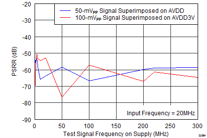
Test Signal Frequency
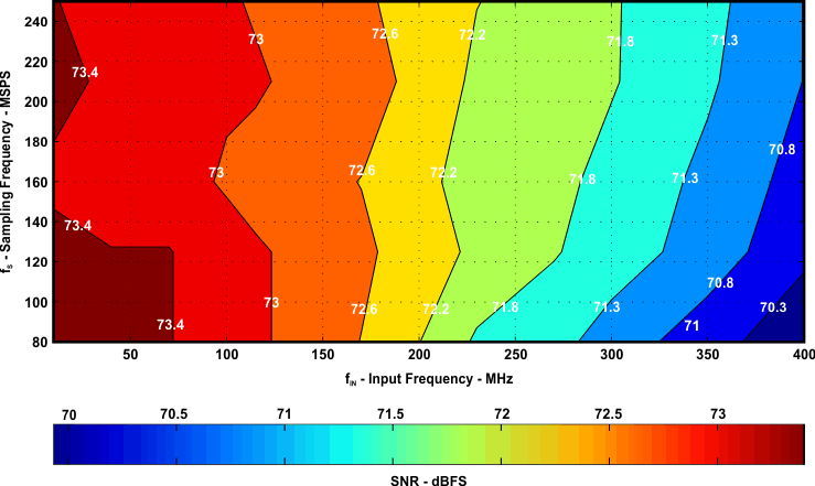
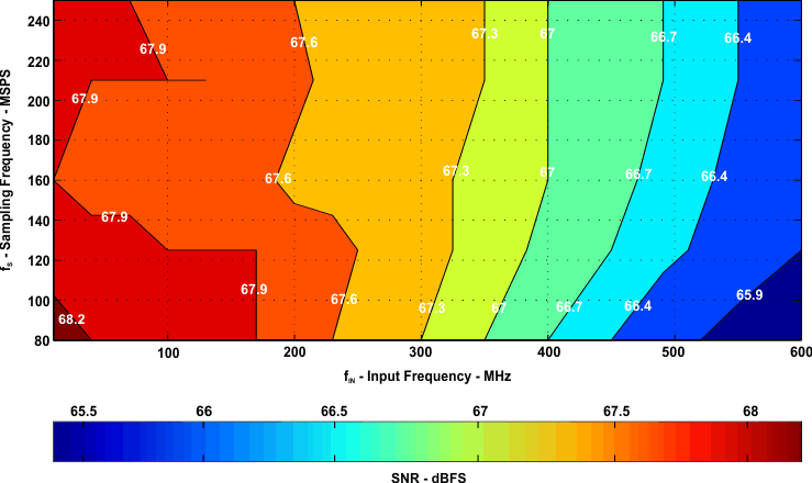
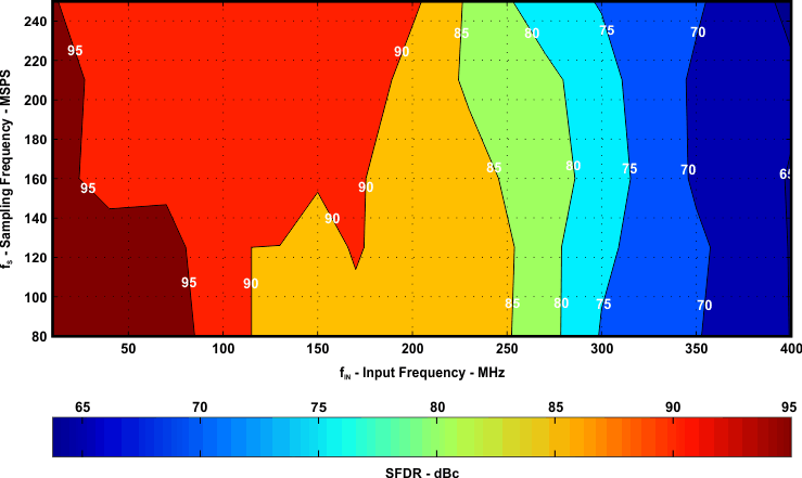
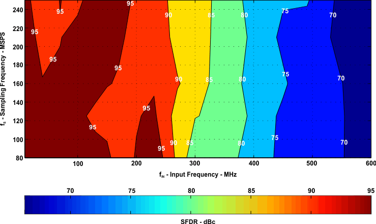
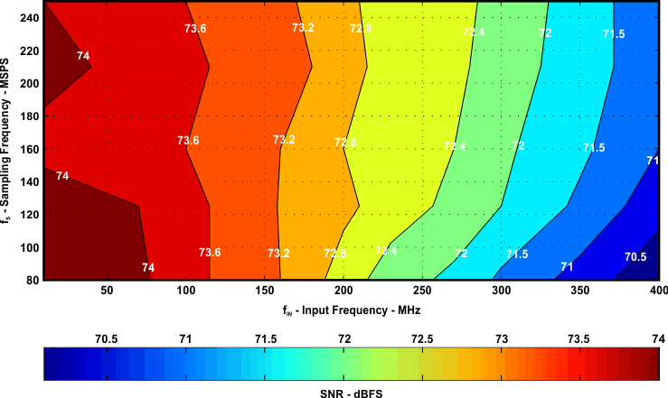
7.13 Typical Characteristics: Contour
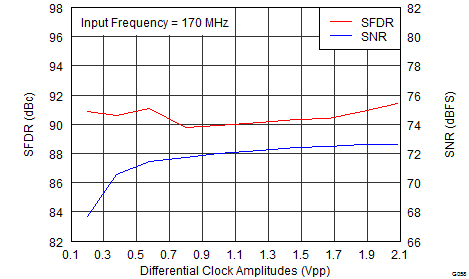
Typical values are at TA = +25°C, full temperature range is TMIN = –40°C to TMAX = +85°C, ADC sampling rate = 250 MSPS, 50% clock duty cycle, AVDD = 1.8 V, AVDD3V = 3.3 V, DRVDD = 1.8 V, IOVDD = 1.8 V, –1-dBFS differential input, 2-VPP full-scale, and 64k-point FFT, unless otherwise noted.7.13.1 Spurious-Free Dynamic Range (SFDR): General
7.13.2 Signal-to-Noise Ratio (SNR): ADS42JB69
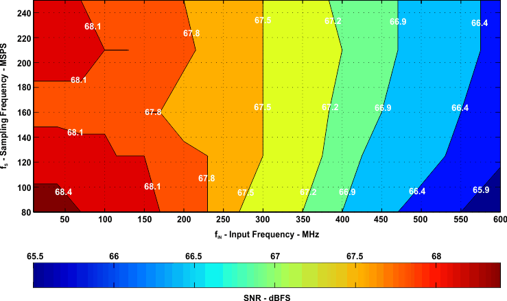
7.13.3 Signal-to-Noise Ratio (SNR): ADS42JB49