SLWS207B May 2008 – January 2016 ADS5560 , ADS5562
PRODUCTION DATA.
- 1 Features
- 2 Applications
- 3 Description
- 4 Revision History
- 5 Pin Configuration and Functions
-
6 Specifications
- 6.1 Absolute Maximum Ratings
- 6.2 ESD Ratings
- 6.3 Recommended Operating Conditions
- 6.4 Thermal Information
- 6.5 Electrical Characteristics
- 6.6 AC Electrical Characteristics for ADS5560 Fs = 40 MSPS
- 6.7 AC Electrical Characteristics for ADS5562, Fs = 80 MSPS
- 6.8 Electrical Characteristics for ADS5562
- 6.9 Electrical Characteristics for ADS5560
- 6.10 Digital Characteristics
- 6.11 Timing Characteristics for LVDS and CMOS Modes
- 6.12 Serial Interface Timing Characteristics
- 6.13 Reset Timing
- 6.14 Timing Characteristics at Lower Sampling Frequencies
- 6.15 Typical Characteristics
- 7 Detailed Description
- 8 Application and Implementation
- 9 Power Supply Recommendations
- 10Layout
- 11Device and Documentation Support
- 12Mechanical, Packaging, and Orderable Information
パッケージ・オプション
メカニカル・データ(パッケージ|ピン)
- RGZ|48
サーマルパッド・メカニカル・データ
- RGZ|48
発注情報
6 Specifications
6.1 Absolute Maximum Ratings
over operating free-air temperature range (unless otherwise noted)(1)| MIN | MAX | UNIT | |||
|---|---|---|---|---|---|
| Supply voltage | AVDD | –0.3 | 3.9 | V | |
| DRVDD | –0.3 | 3.9 | V | ||
| Voltage between AGND and DRGND | –0.3 | 0.3 | V | ||
| Voltage between AVDD and DRVDD | –0.3 | 3.3 | V | ||
| Voltage applied to VCM pin (in external reference mode) | –0.3 | 1.8 | V | ||
| Voltage applied to analog input pins | INP, INM | –0.3 | (3.6, AVDD + 0.3 ) | V | |
| CLKP, CLKM(2), MODE | –0.3 | (3.6, AVDD + 0.3 ) | |||
| RESET, SCLK, SDATA, SEN, OE, DFS | –0.3 | (3.6, DRVDD + 0.3 ) | V | ||
| TA | Operating free-air temperature | –40 | 85 | °C | |
| Tjmax | Operating junction temperature | 125 | °C | ||
| Lead temperature 1,6 mm (1/16") from the case for 10 s | 220 | °C | |||
| TSTG | Storage temperature | –65 | 150 | °C | |
(1) Stresses beyond those listed under Absolute Maximum Ratings may cause permanent damage to the device. These are stress ratings only, which do not imply functional operation of the device at these or any other conditions beyond those indicated under Recommended Operating Conditions. Exposure to absolute-maximum-rated conditions for extended periods may affect device reliability.
(2) When AVDD is turned off, TI recommends switching off the input clock (or ensure the voltage on CLKP, CLKM is <|0.3 V|). This prevents the ESD protection diodes at the clock input pins from turning on.
6.2 ESD Ratings
| VALUE | UNIT | |||
|---|---|---|---|---|
| V(ESD) | Electrostatic discharge | Human-body model (HBM), per ANSI/ESDA/JEDEC JS-001(1) | 2000 | V |
| Charged-device model (CDM), per JEDEC specification JESD22-C101(2) | 500 | |||
(1) JEDEC document JEP155 states that 500-V HBM allows safe manufacturing with a standard ESD control process.
(2) JEDEC document JEP157 states that 250-V CDM allows safe manufacturing with a standard ESD control process.
6.3 Recommended Operating Conditions
over operating free-air temperature range (unless otherwise noted)| MIN | NOM | MAX | UNIT | ||||
|---|---|---|---|---|---|---|---|
| SUPPLIES AND REFERENCES | |||||||
| AVDD | Analog supply voltage | 3 | 3.3 | 3.6 | V | ||
| DRVDD | Digital supply voltage | 3 | 3.3 | 3.6 | V | ||
| ANALOG INPUTS | |||||||
| Differential input voltage range (with default fine gain=1 dB) | 3.56 | VPP | |||||
| Input common-mode voltage | 1.5 ±0.1 | V | |||||
| Voltage applied on VCM in external reference mode | 1.5 ±0.05 | V | |||||
| CLOCK INPUT | |||||||
| Sample rate | ADS5562 | DEFAULT SPEED mode | > 25 | 80 | MSPS | ||
| LOW SPEED mode(2) | 1 | 25 | MSPS | ||||
| ADS5560 | DEFAULT SPEED mode | > 25 | 40 | MSPS | |||
| LOW SPEED mode | 1 | 25 | MSPS | ||||
| Clock amplitude, ac-coupled, differential (VCLKP – VCLKM)(1) | 0.4 | VPP | |||||
| Clock duty cycle | 45% | 50% | 55% | ||||
| DIGITAL OUTPUTS | |||||||
| CL | Maximum external load capacitance from each output pin to DRGND (LVDS and CMOS modes) | 5 | pF | ||||
| RL | Differential external load resistance between the LVDS output pairs (LVDS mode) | 100 | Ω | ||||
| Operating free-air temperature | –40 | 85 | °C | ||||
(1) Supported clock waveform formats: sine wave, LVPECL, LVDS, and LVCMOS
(2) See the Low Sampling Frequency Operation section for details.
6.4 Thermal Information
| THERMAL METRIC(1) | ADS5560 ADS5562 |
UNIT | |
|---|---|---|---|
| RGZ (VQFN) | |||
| 48 PINS | |||
| RθJA | Junction-to-ambient thermal resistance | 27.6 | °C/W |
| RθJC(top) | Junction-to-case (top) thermal resistance | 12.4 | °C/W |
| RθJB | Junction-to-board thermal resistance | 4.4 | °C/W |
| ψJT | Junction-to-top characterization parameter | 0.2 | °C/W |
| ψJB | Junction-to-board characterization parameter | 4.4 | °C/W |
| RθJC(bot) | Junction-to-case (bottom) thermal resistance | 0.9 | °C/W |
(1) For more information about traditional and new thermal metrics, see the Semiconductor and IC Package Thermal Metrics application report, SPRA953.
6.5 Electrical Characteristics
Typical values are at 25°C, AVDD = DRVDD = 3.3 V, sampling rate = Maximum Rated, sine wave input clock, 1.5-VPP clock amplitude, 50% clock duty cycle, –1-dBFS differential analog input, internal reference mode, DDR LVDS interface, default fine gain (1 dB). Minimum and maximum values are across the full temperature range TMIN = –40°C to TMAX = 85°C, AVDD = DRVDD = 3.3 V, sampling rate = Maximum Rated, unless otherwise noted.| PARAMETER | TEST CONDITIONS | MIN | TYP | MAX | UNIT | ||
|---|---|---|---|---|---|---|---|
| Resolution | 16 | bits | |||||
| ANALOG INPUT | |||||||
| Differential input voltage range (1) | 3.56 | VPP | |||||
| Differential input capacitance | 5 | pF | |||||
| Analog input bandwidth | 300 | MHz | |||||
| Analog input common-mode current (per input pin) | 6.6 | μA/MSPS | |||||
| VCM | Common-mode output voltage | Internal reference mode | 1.5 | V | |||
| VCM output current capability | Internal reference mode | ±4 | mA | ||||
| DC ACCURACY | |||||||
| No Missing Codes | 0-dB gain | Assured | |||||
| DNL | Differential non-linearity | –0.95 | 0.5 | 3 | LSB | ||
| INL | Integral non-linearity | –8.5 | ±3 | 8.5 | LSB | ||
| Offset error | –25 | ±10 | 25 | mV | |||
| Offset error temperature coefficient | 0.005 | mV/°C | |||||
| Variation of offset error across AVDD supply | 1.5 | mV/V | |||||
| There are two sources of gain error: I) internal reference inaccuracy and ii) channel gain error | |||||||
| EGREF | Gain error due to internal reference inaccuracy alone | –2.5 | ±1 | 2.5 | % full scale | ||
| ECHAN | Channel gain error alone | –2.5 | ± 1 | 2.5 | % full scale | ||
| Channel gain error temperature coefficient | 0.01 | Δ%/°C | |||||
| POWER SUPPLY | |||||||
| IAVDD | Analog supply current | ADS5560 | 210 | 250 | mA | ||
| ADS5562 | 160 | 190 | |||||
| IDRVDD | Digital supply current | LVDS mode CL = 5 pF, IO = 3.5 mA, RL = 100 Ω |
ADS5560 | 52 | mA | ||
| ADS5562 | 44 | ||||||
| CMOS mode CL = 5 pF, FIN = 3 MHz |
ADS5560 | 60 | mA | ||||
| ADS5562 | 37 | ||||||
| Total power | LVDS mode | ADS5560 | 865 | 1100 | mW | ||
| ADS5562 | 674 | 810 | |||||
| Standby power | STANDBY mode with clock running | ADS5560 | 155 | mW | |||
| ADS5562 | 135 | ||||||
| Clock stop power | 125 | 150 | mW | ||||
(1) The full-scale voltage range is a function of the fine gain settings. See Table 1.
6.6 AC Electrical Characteristics for ADS5560 Fs = 40 MSPS
Typical values are at 25°C, AVDD = DRVDD = 3.3 V, sampling rate = Maximum Rated, sine wave input clock, 1.5-VPP clock amplitude, 50% clock duty cycle, –1-dBFS differential analog input, internal reference mode, DDR LVDS interface, 0 dB fine gain(1). Minimum and maximum values are across the full temperature range TMIN = –40°C to TMAX = 85°C, AVDD = DRVDD = 3.3 V, sampling rate = Maximum Rated, default fine gain (1 dB), unless otherwise noted.| PARAMETER | TEST CONDITIONS | MIN | TYP | MAX | UNIT | |
|---|---|---|---|---|---|---|
| SNR Signal to noise ratio |
LVDS interface | FIN = 3 MHz | 84.3 | dBFS | ||
| FIN = 10 MHz | 80 | 84 | ||||
| FIN = 25 MHz | 82.5 | |||||
| FIN = 30 MHz | 81.8 | |||||
| CMOS interface | FIN = 3 MHz | 83.5 | dBFS | |||
| FIN = 10 MHz | 78 | 83.1 | ||||
| FIN = 25 MHz | 81.8 | |||||
| FIN = 30 MHz | 81.6 | |||||
| RMS output noise | Inputs tied to common-mode | 1.42 | LSB | |||
| SINAD Signal to noise and distortion ratio |
LVDS interface | FIN = 3 MHz | 83.2 | dBFS | ||
| FIN = 10 MHz | 76 | 83 | ||||
| FIN = 25 MHz | 79 | |||||
| FIN = 30 MHz | 77 | |||||
| CMOS interface | FIN = 3 MHz | 82 | dBFS | |||
| FIN = 10 MHz | 75 | 81.4 | ||||
| FIN = 25 MHz | 79.3 | |||||
| FIN = 30 MHz | 78 | |||||
| ENOB Effective number of bits |
LVDS interface, FIN = 10 MHz | 12.4 | 13.5 | bits | ||
| SFDR Spurious free dynamic range |
FIN = 3 MHz | 90 | dBc | |||
| FIN = 10 MHz | 78 | 88 | ||||
| FIN = 25 MHz | 83 | |||||
| FIN = 30 MHz | 79 | |||||
| HD2 Second harmonic |
FIN = 3 MHz | 94 | dBc | |||
| FIN = 10 MHz | 78 | 92 | ||||
| FIN = 25 MHz | 90 | |||||
| FIN = 30 MHz | 88 | |||||
(1) After reset, the device is initialized to 1-dB fine gain setting. For SFDR and SNR performance across fine gains, see the Typical Characteristics section.
6.7 AC Electrical Characteristics for ADS5562, Fs = 80 MSPS
Typical values are at 25°C, AVDD = DRVDD = 3.3 V, sampling rate = Maximum Rated, sine wave input clock, 1.5-VPP clock amplitude, 50% clock duty cycle, –1-dBFS differential analog input, internal reference mode, DDR LVDS interface, 0 dB fine gain(1). Minimum and maximum values are across the full temperature range TMIN = –40°C to TMAX = 85°C, AVDD = DRVDD = 3.3 V, sampling rate = Maximum Rated, default fine gain (1 dB), unless otherwise noted.| PARAMETER | TEST CONDITIONS | MIN | TYP | MAX | UNIT | |
|---|---|---|---|---|---|---|
| SNR Signal to noise ratio |
LVDS interface | FIN = 3 MHz | 84 | dBFS | ||
| FIN = 10 MHz | 79 | 83.8 | ||||
| FIN = 25 MHz | 83.2 | |||||
| FIN = 30 MHz | 82.8 | |||||
| CMOS interface | FIN = 3 MHz | 81.7 | dBFS | |||
| FIN = 10 MHz | 77 | 81.4 | ||||
| FIN = 25 MHz | 80.7 | |||||
| FIN = 30 MHz | 80.4 | |||||
| RMS output noise | Inputs tied to common-mode | 1.42 | LSB | |||
| SINAD Signal to noise and distortion ratio |
LVDS interface | FIN = 3 MHz | 80.5 | dBFS | ||
| FIN = 10 MHz | 75 | 80.5 | ||||
| FIN = 25 MHz | 79.5 | |||||
| FIN = 30 MHz | 79 | |||||
| CMOS interface | FIN = 3 MHz | 80.5 | dBFS | |||
| FIN = 10 MHz | 73.5 | 80.2 | ||||
| FIN = 25 MHz | 79.3 | |||||
| FIN = 30 MHz | 77.9 | |||||
| ENOB Effective number of bits |
LVDS interface, FIN = 10 MHz | 12.2 | 13.1 | bits | ||
| SFDR Spurious free dynamic range |
FIN = 3 MHz | 85 | dBc | |||
| FIN = 10 MHz | 77 | 85 | ||||
| FIN = 25 MHz | 83 | |||||
| FIN = 30 MHz | 80 | |||||
| HD2 Second harmonic |
FIN = 3 MHz | 90 | dBc | |||
| FIN = 10 MHz | 77 | 89 | ||||
| FIN = 25 MHz | 88 | |||||
| FIN = 30 MHz | 88 | |||||
6.8 Electrical Characteristics for ADS5562
Typical values are at 25°C, AVDD = DRVDD = 3.3 V, sampling rate = Maximum Rated, sine wave input clock, 1.5-VPP clock amplitude, 50% clock duty cycle, –1-dBFS differential analog input, 0 dB fine gain(1), internal reference mode, DDR LVDS interface. Minimum and maximum values are across the full temperature range TMIN = –40°C to TMAX = 85°C, AVDD = DRVDD = 3.3 V, sampling rate = Maximum Rated, default fine gain (1 dB), unless otherwise noted.| PARAMETER | TEST CONDITIONS | MIN | TYP | MAX | UNIT | |
|---|---|---|---|---|---|---|
| HD3 Third harmonic |
FIN = 3 MHz | 85 | dBc | |||
| FIN = 10 MHz | 77 | 85 | ||||
| FIN = 25 MHz | 83 | |||||
| FIN = 30 MHz | 80 | |||||
| Worst harmonic other than HD2, HD3 |
FIN = 3 MHz | 104 | dBc | |||
| FIN = 10 MHz | 102 | |||||
| FIN = 25 MHz | 100 | |||||
| FIN = 30 MHz | 100 | |||||
| THD Total harmonic distortion |
FIN = 3 MHz | 84 | dBc | |||
| FIN = 10 MHz | 75.5 | 83 | ||||
| FIN = 25 MHz | 82 | |||||
| FIN = 30 MHz | 80 | |||||
| IMD Two-tone intermodulation distortion |
FIN1 = 5 MHz, FIN2 = 10 MHz, each tone –7 dBFS | 92 | dBFS | |||
| Voltage overload recovery time | Recovery to 1% for 6-dB overload | 1 | clock cycles | |||
(1) After reset, the device is initialized to 1-dB fine gain setting. For SFDR and SNR performance across fine gains, see the Typical Characteristics section.
6.9 Electrical Characteristics for ADS5560
Typical values are at 25°C, AVDD = DRVDD = 3.3 V, sampling rate = Maximum Rated, sine wave input clock, 1.5-VPP clock amplitude, 50% clock duty cycle, –1-dBFS differential analog input, internal reference mode, DDR LVDS interface, 0 dB fine gain(1). Minimum and maximum values are across the full temperature range TMIN = –40°C to TMAX = 85°C, AVDD = DRVDD = 3.3 V, sampling rate = Maximum Rated, default fine gain (1 dB), unless otherwise noted.| PARAMETER | TEST CONDITIONS | MIN | TYP | MAX | UNIT | |
|---|---|---|---|---|---|---|
| HD3 Third harmonic |
FIN = 3 MHz | 90 | dBc | |||
| FIN = 10 MHz | 78 | 88 | ||||
| FIN = 25 MHz | 83 | |||||
| FIN = 30 MHz | 79 | |||||
| Worst harmonic other than HD2, HD3 |
FIN = 3 MHz | 104 | dBc | |||
| FIN = 10 MHz | 102 | |||||
| FIN = 25 MHz | 101 | |||||
| FIN = 30 MHz | 101 | |||||
| THD Total harmonic distortion |
FIN = 3 MHz | 88 | dBc | |||
| FIN = 10 MHz | 76.5 | 86 | ||||
| FIN = 25 MHz | 81 | |||||
| FIN = 30 MHz | 78 | |||||
| IMD Two-tone intermodulation distortion |
FIN1 = 5 MHz, FIN2 = 10 MHz, each tone –7 dBFS | 98 | dBFS | |||
| Voltage overload recovery time | Recovery to 1% for 6-dB overload | 1 | clock cycles | |||
6.10 Digital Characteristics
DC specifications refer to the condition where the digital outputs are not switching, but are permanently at a valid logic level 0 or 1, AVDD = 3 V to 3.6 V, IO = 3.5 mA, RL = 100 Ω(1)(2)| PARAMETER | TEST CONDITIONS | MIN | TYP | MAX | UNIT |
|---|---|---|---|---|---|
| DIGITAL INPUTS | |||||
| High-level input voltage | 2.4 | V | |||
| Low-level input voltage | 0.8 | V | |||
| High-level input current | 33 | μA | |||
| Low-level input current | –33 | μA | |||
| Input capacitance | 4 | pF | |||
| DIGITAL OUTPUTS – CMOS MODE | |||||
| High-level output voltage | DRVDD | V | |||
| Low-level output voltage | 0 | V | |||
| Output capacitance | Capacitance inside the device from each output pin to ground | 4 | pF | ||
| DIGITAL OUTPUTS – LVDS MODE | |||||
| High-level output voltage, VODH | 350 | mV | |||
| Low-level output voltage, VODL | –350 | mV | |||
| Output common-mode voltage, VOCM | 1.2 | V | |||
| Output capacitance | Capacitance inside the device from each output pin to ground | 4 | pF | ||
(1) All LVDS and CMOS specifications are characterized, but not tested at production.
(2) IO refers to the LVDS buffer current setting; RL is the differential load resistance between the LVDS output pair.
6.11 Timing Characteristics for LVDS and CMOS Modes
Typical values are at 25°C, AVDD = 3.3 V, DRVDD = 3 to 3.6 V, Sampling frequency = 80 MSPS, sine wave input clock, 50% clock duty cycle, 1.5-VPP clock amplitude, CL = 5 pF(2) , no internal termination, IO = 3.5 mA, RL = 100 Ω(3) Minimum and maximum values are across the full temperature range TMIN = –40°C to TMAX = 85°C, AVDD = DRVDD = 3 to 3.6 V, unless otherwise noted.(1)| MIN | NOM | MAX | UNIT | ||||
|---|---|---|---|---|---|---|---|
| ta | Aperture delay | 0.5 | 1.2 | 2 | ns | ||
| tj | Aperture jitter | Sampling frequency = 80 MSPS | 90 | fs rms | |||
| Sampling frequency = 40 MSPS | 135 | fs rms | |||||
| Wake-up time | Time to data stable(8) after coming out of STANDBY mode | 60 | 200 | μs | |||
| Time to valid data after stopping and restarting the input clock | 80 | μs | |||||
| Latency | 16 | Clock cycles | |||||
| DDR LVDS MODE(4) | |||||||
| LVDS bit clock duty cycle | 47% | 50% | 53% | ||||
| tsu | Data setup time(5) | Data valid(6) to zero-crossing of CLKOUTP | 2 | 3 | ns | ||
| th | Data hold time(5) | Zero-crossing of CLKOUTP to data becoming invalid(6) | 2 | 3 | ns | ||
| tPDI | Clock propagation delay | Input clock rising edge cross-over to output clock rising edge cross-over | 9.5 | 11 | 12.5 | ns | |
| tr | Data rise time | Rise time measured from –100 mV to 100 mV | 0.15 | 0.22 | 0.3 | ns | |
| tf | Data fall time | Fall time measured from 100 mV to –100 mV | 0.15 | 0.22 | 0.3 | ns | |
| tr | Output clock rise time | Rise time measured from –100 mV to 100 mV | 0.15 | 0.22 | 0.3 | ns | |
| tf | Output clock fall time | Fall time measured from 100 mV to –100 mV | 0.15 | 0.22 | 0.3 | ns | |
| tOE | Output enable (OE) to data delay | Time to data valid after OE becomes active | 700 | ns | |||
| PARALLEL CMOS MODE | |||||||
| CMOS output clock duty cycle | 50% | ||||||
| tsu | Data setup time | Data valid(7) to 50% of CLKOUT rising edge | 6.5 | 8 | ns | ||
| th | Data hold time | 50% of CLKOUT rising edge to data becoming invalid (7) | 2 | 3 | ns | ||
| tPDI | Clock propagation delay | Input clock rising edge cross-over to 50% of CLKOUT rising edge | 6.3 | 7.8 | 9.3 | ns | |
| tr | Data rise time | Rise time measured from 20% to 80% of DRVDD | 1 | 1.5 | 2 | ns | |
| tf | Data fall time | Fall time measured from 80% to 20% of DRVDD | 1 | 1.5 | 2 | ns | |
| tr | Output clock rise time | Rise time measured from 20% to 80% of DRVDD | 0.7 | 1 | 1.2 | ns | |
| tf | Output clock fall time | Fall time measured from 80% to 20% of DRVDD | 1.2 | 1.5 | 1.8 | ns | |
| tOE | Output enable (OE) to data delay | Time to data valid after OE becomes active | 200 | ns | |||
(1) Timing parameters are ensured by design and characterization and not tested in production.
(2) CL is the effective external single-ended load capacitance between each output pin and ground.
(3) IO refers to the LVDS buffer current setting; RL is the differential load resistance between the LVDS output pair.
(4) Measurements are done with a transmission line of 100-Ω characteristic impedance between the device and the load.
(5) Setup and hold time specifications take into account the effect of jitter on the output data and clock.
(6) Data valid refers to logic high of 100 mV and logic low of –100 mV.
(7) Data valid refers to logic high of 2.6 V and logic low of 0.66 V.
(8) Data stable is defined as the point at which the SNR is within 2 dB of thenormal value.
6.12 Serial Interface Timing Characteristics
Typical values at 25°C, minimum and maximum values across the full temperature range TMIN = –40°C to TMAX = 85°C, AVDD = DRVDD = 3.3 V (unless otherwise noted)| MIN | NOM | MAX | UNIT | ||
|---|---|---|---|---|---|
| fSCLK | SCLK frequency | > DC | 20 | MHz | |
| tSLOADS | SEN to SCLK setup time | 25 | ns | ||
| tSLOADH | SCLK to SEN hold time | 25 | ns | ||
| tDSU | SDATA setup time | 25 | ns | ||
| tDH | SDATA hold time | 25 | ns | ||
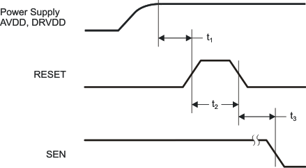
6.13 Reset Timing
Typical values at 25°C, minimum and maximum values across the full temperature range TMIN = –40°C to TMAX = 85°C, AVDD = DRVDD = 3.3 V (unless otherwise noted)| MIN | NOM | MAX | UNIT | |||
|---|---|---|---|---|---|---|
| t1 | Power-on delay | Delay from power-up of AVDD and DRVDD to RESET pulse active | 5 | ms | ||
| t2 | Reset pulse width | Pulse width of active RESET signal | 10 | ns | ||
| 1 | μs | |||||
| t3 | Register write delay | Delay from RESET disable to SEN active | 25 | ns | ||
| tPO | Power-up time | Delay from power-up of AVDD and DRVDD to output stable | 6.5 | ms | ||
6.14 Timing Characteristics at Lower Sampling Frequencies
NOTE:
A high-going pulse on RESET pin is required in serial interface mode in case of initialization through hardware reset. If the pulse is greater than 1 µs, the device could enter the parallel configuration mode briefly then return back to serial interface mode. For parallel interface operation, RESET must be tied permanently HIGH.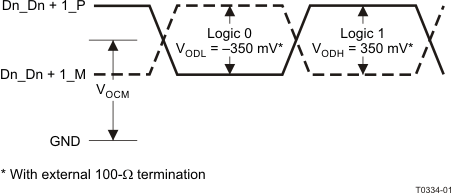 Figure 2. LVDS Output Voltage Levels
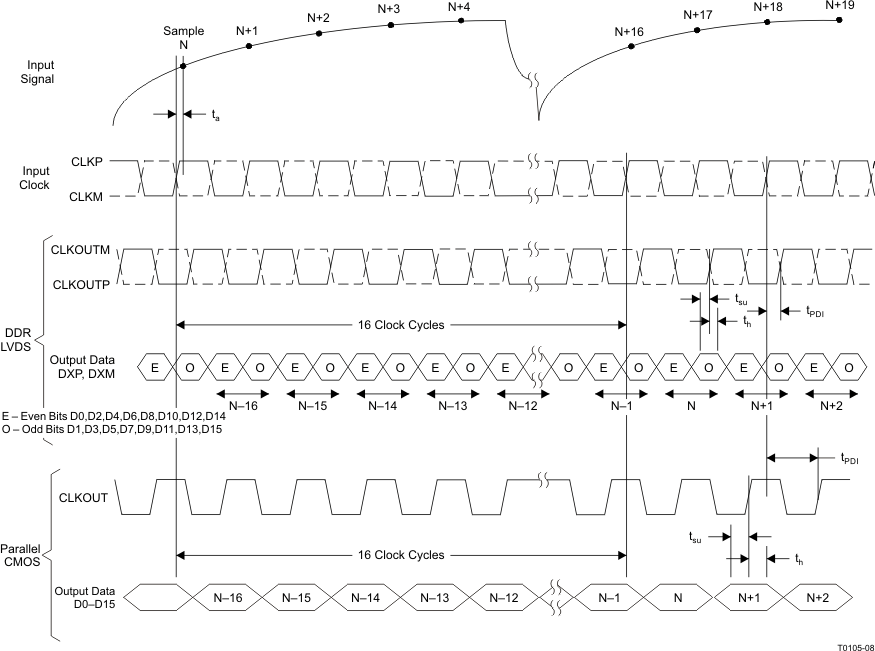 Figure 3. Latency
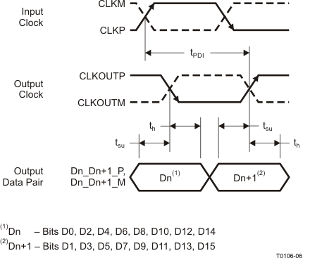 Figure 4. LVDS Mode Timing
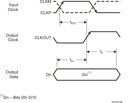 Figure 5. CMOS Mode Timing
6.15 Typical Characteristics
6.15.1 ADS5562 – 80 MSPS
Typical values are at 25°C, AVDD = DRVDD = 3.3 V, sampling frequency = Maximum Rated, sine wave input clock, 1.5-VPP clock amplitude, 50% clock duty cycle, –1-dBFS differential analog input, internal reference mode, DDR LVDS interface, default fine gain (1 dB), 32k Point FFT (unless otherwise noted)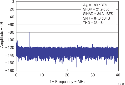 Figure 8. FFT for 5 MHz, –80-dBFS Input Signal (Small Signal)
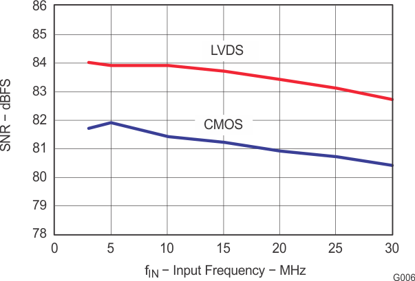 Figure 10. SNR vs Fin, 0-dB Gain
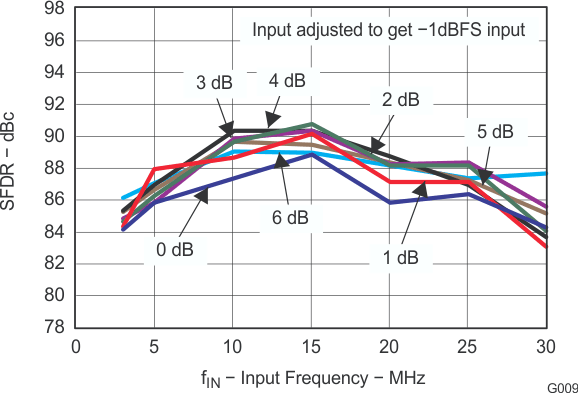 Figure 12. SFDR Across Fine Gain
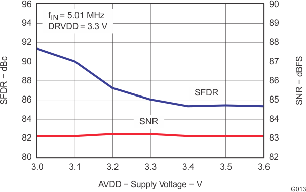 Figure 14. Performance vs AVDD Supply
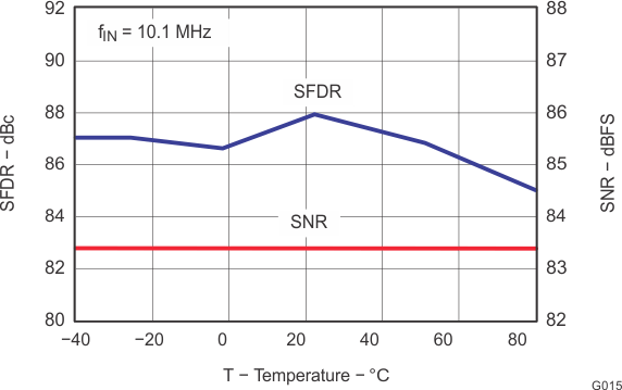 Figure 16. Performance vs Temperature
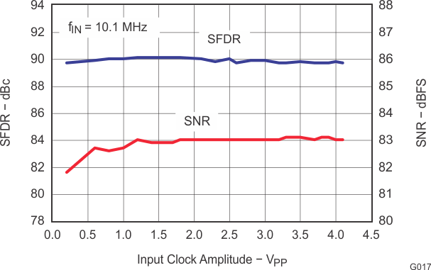 Figure 18. Performance vs Clock Amplitude
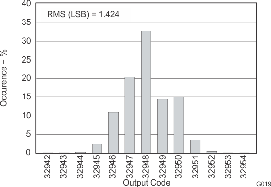 Figure 20. Output Noise Histogram
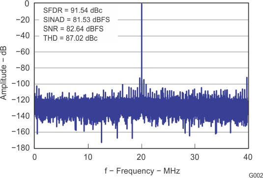 Figure 7. FFT for 20 MHz, –1-dBFS Input Signal
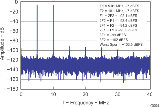 Figure 9. Intermodulation Distortion
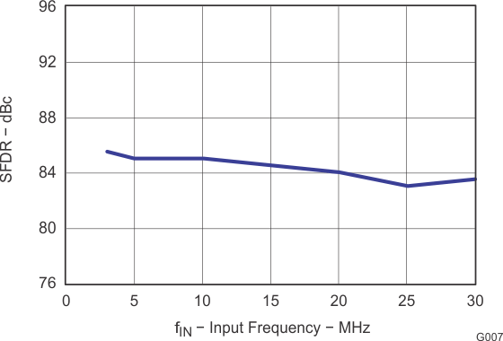 Figure 11. SFDR vs FIN
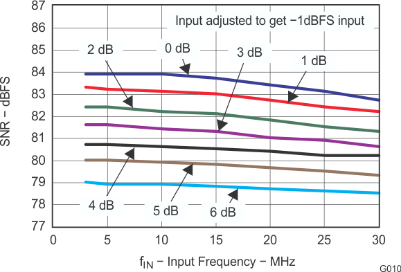 Figure 13. SNR Across Fine Gain
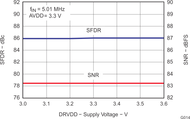 Figure 15. Performance vs DRVDD Supply
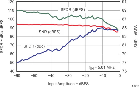 Figure 17. Performance vs Input Amplitude, 0-dB Gain
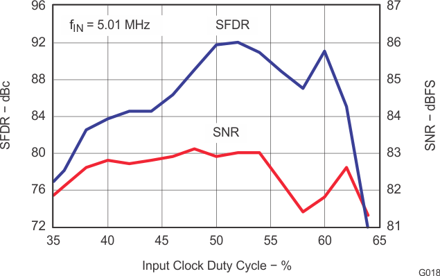 Figure 19. Performance vs Clock Duty Cycle
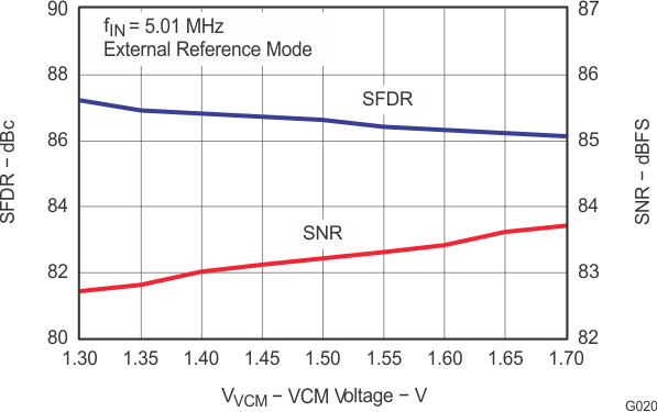 Figure 21. Performance in External Reference Mode
6.15.2 ADS5560 – 40 MSPS
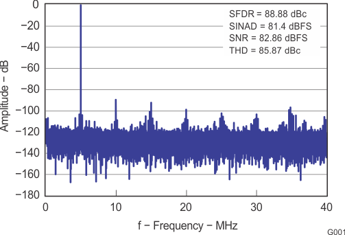
Typical values are at 25°C, AVDD = DRVDD = 3.3 V, sampling frequency = Maximum Rated, sine wave input clock, 1.5-VPP clock amplitude, 50% clock duty cycle, –1-dBFS differential analog input, internal reference mode, DDR LVDS interface, default fine gain (1 dB), 32k Point FFT (unless otherwise noted)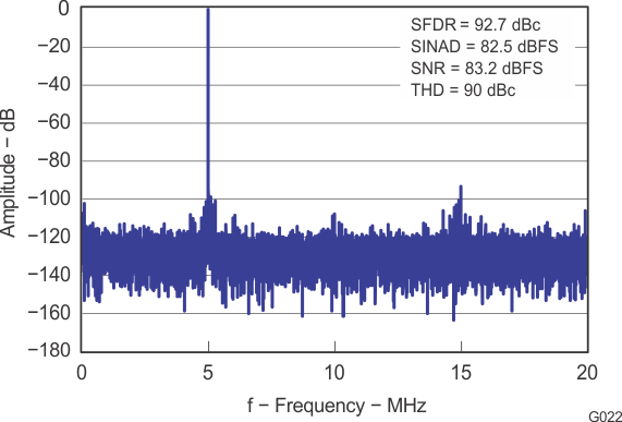 Figure 22. FFT for 5 MHz, –1-dBFS Input Signal
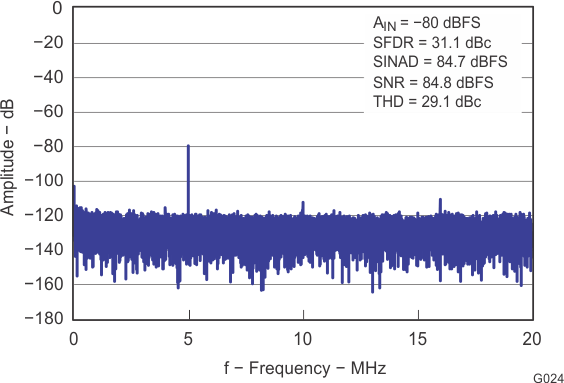 Figure 24. FFT for 5 MHz, –80-dBFS Input Signal
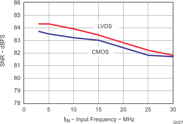 Figure 26. SNR vs Fin, 0-dB Gain
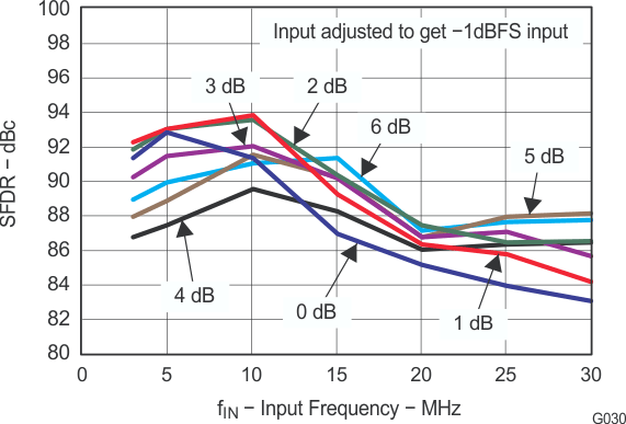 Figure 28. SFDR Across Fine Gain
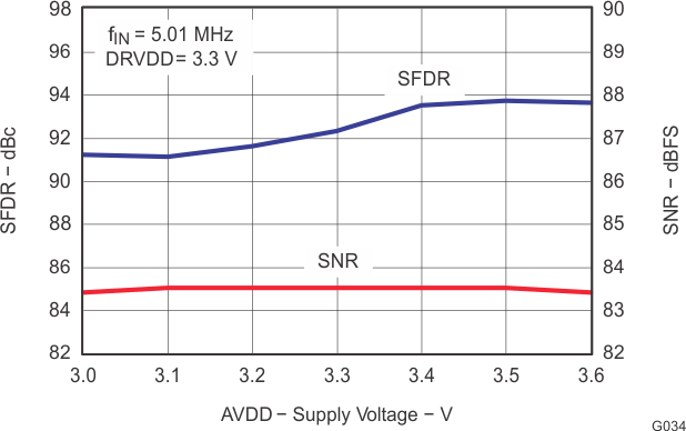 Figure 30. Performance vs AVDD Supply
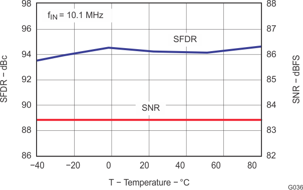 Figure 32. Performance vs Temperature
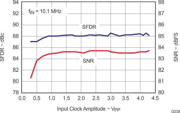 Figure 34. Performance vs Clock Amplitude
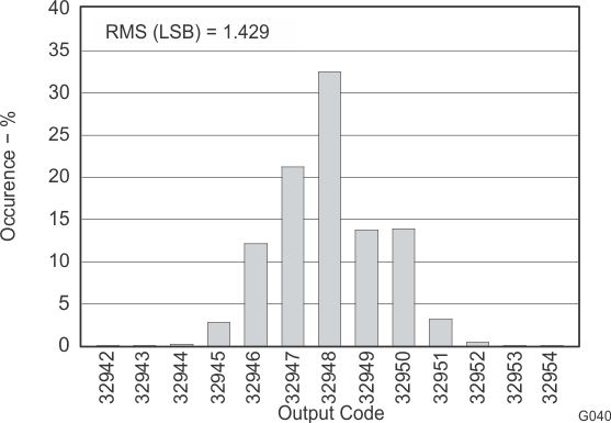 Figure 36. Output Noise Histogram
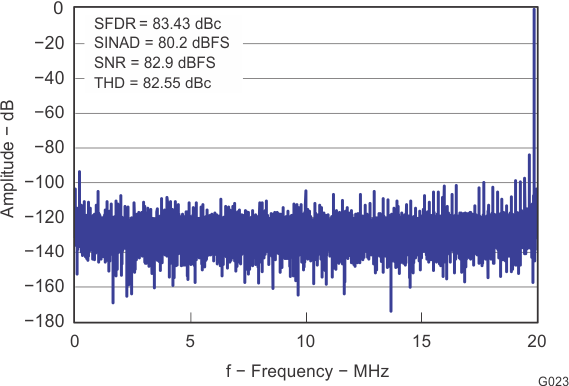 Figure 23. FFT for 20 MHz, –1-dBFS Input Signal
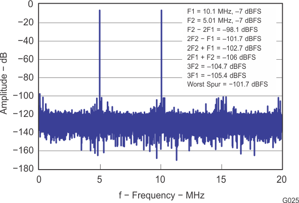 Figure 25. Intermodulation Distortion
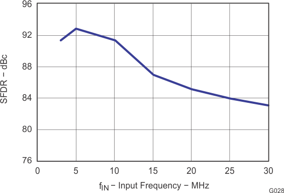 Figure 27. SFDR vs Fin
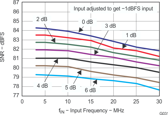 Figure 29. SNR Across Fine Gain
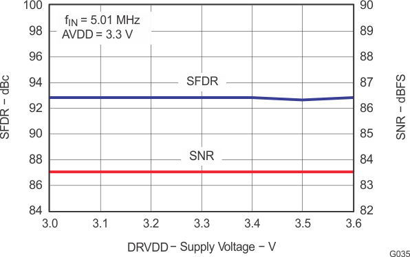 Figure 31. Performance vs DRVDD Supply
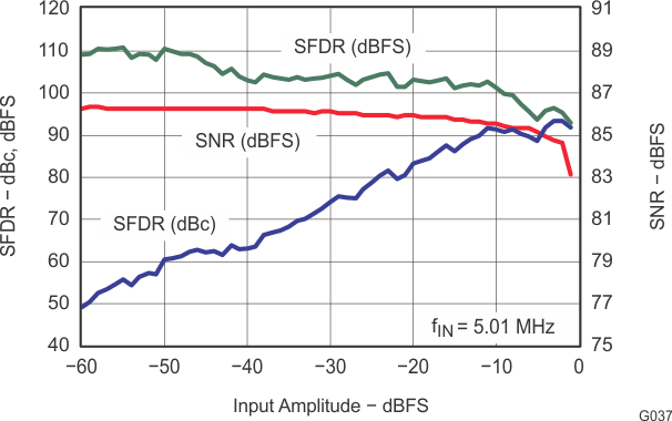 Figure 33. Performance vs Input Amplitude, 0-dB Gain
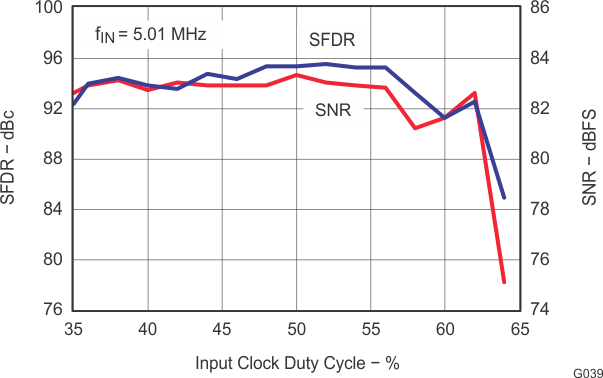 Figure 35. Performance vs Clock Duty Cycle
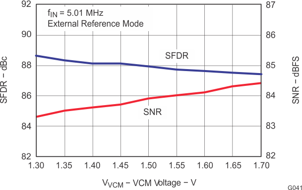 Figure 37. Performance in External Reference Mode
6.15.3 Valid Up to Max Clock Rate (ADS5562 or ADS5560)
Typical values are at 25°C, AVDD = DRVDD = 3.3 V, sampling frequency = Maximum Rated, sine wave input clock, 1.5-VPP clock amplitude, 50% clock duty cycle, –1-dBFS differential analog input, internal reference mode, DDR LVDS interface, default fine gain (1 dB), 32k Point FFT (unless otherwise noted)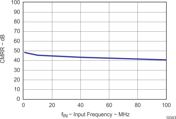 Figure 38. CMRR vs Common-Mode Frequency
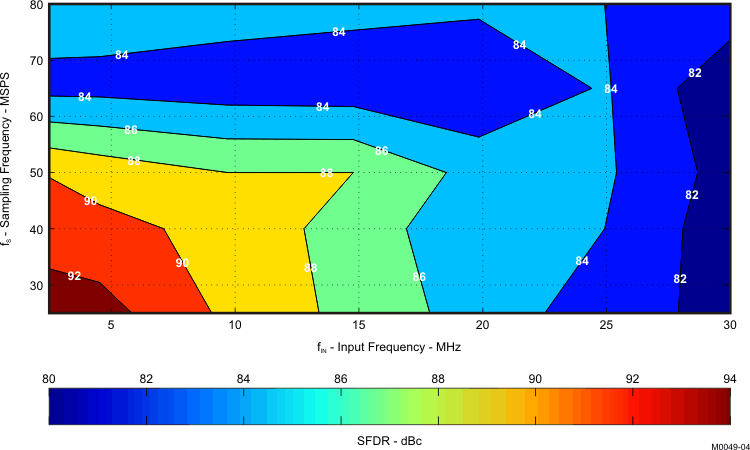 Figure 40. SFDR Contour, 0-dB Gain
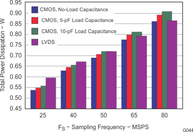 Figure 39. Power Dissipation vs Sampling Frequency
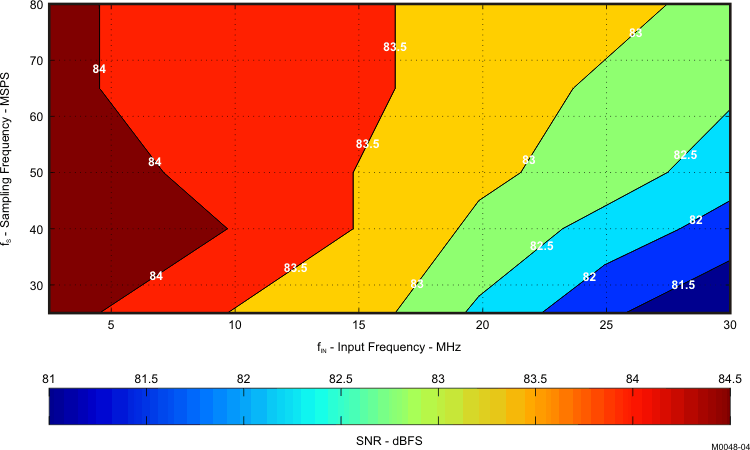 Figure 41. SNR Contour, 0-dB Gain
