SBAS717A June 2015 – June 2015 ADS58J63
PRODUCTION DATA.
- 1 Features
- 2 Applications
- 3 Description
- 4 Revision History
- 5 Pin Configuration and Functions
-
6 Specifications
- 6.1 Absolute Maximum Ratings
- 6.2 ESD Ratings
- 6.3 Recommended Operating Conditions
- 6.4 Thermal Information
- 6.5 Electrical Characteristics
- 6.6 AC Performance
- 6.7 Digital Characteristics
- 6.8 Timing Characteristics
- 6.9 Typical Characteristics: 14-Bit Burst Mode
- 6.10 Typical Characteristics: Mode 2
- 6.11 Typical Characteristics: Mode 0
-
7 Detailed Description
- 7.1 Overview
- 7.2 Functional Block Diagram
- 7.3 Feature Description
- 7.4
Device Functional Modes
- 7.4.1 Digital Features
- 7.4.2 Mode 0 - Decimation by 2 with IQ Outputs for up to 220 MHz of IQ Bandwidth
- 7.4.3 Mode 2 - Decimation by 2 for up to 110 MHz of Real Bandwidth
- 7.4.4 Mode 4/7 - Decimation by 2 with Real Outputs for up to 110 MHz of Bandwidth
- 7.4.5 Mode 5 - Decimation by 2 with IQ Outputs for up to 110 MHz of IQ Bandwidth
- 7.4.6 Mode 6 - Decimation by 4 with IQ Outputs for up to 110 MHz of IQ Bandwidth
- 7.4.7 Mode 8 - Burst Mode
- 7.4.8 Trigger Input
- 7.4.9 Manual Trigger Mode
- 7.4.10 Auto Trigger Mode
- 7.4.11 Over-range Indication
- 7.4.12 Power-Down Mode
- 7.5
Programming
- 7.5.1
Device Configuration
- 7.5.1.1 Details of Serial Interface
- 7.5.1.2 Serial Register Write: Analog Bank
- 7.5.1.3 Serial Register Readout: Analog Bank
- 7.5.1.4 JESD Bank SPI Page Selection
- 7.5.1.5 Serial Register Write: Analog Bank
- 7.5.1.6 Serial Register Readout: Analog Bank
- 7.5.1.7 Digital Bank SPI Page Selection
- 7.5.1.8 Serial Register Write - Digital Bank
- 7.5.1.9 Individual Channel Programming
- 7.5.1.10 Serial Register Readout - Digital Bank
- 7.5.2 JESD204B Interface
- 7.5.1
Device Configuration
- 7.6
Register Maps
- 7.6.1 Detailed Register Info
- 7.6.2 Example Register Writes
- 7.6.3
Register Descriptions
- 7.6.3.1 Register 0h (offset = 0h) [reset = 0h]
- 7.6.3.2 Register 3h/4h (offset = 3h/4h) [reset = 0h]
- 7.6.3.3 Register 5h (offset = 5h) [reset = 0h]
- 7.6.3.4 Register 11h (offset = 11h) [reset = 0h]
- 7.6.3.5
Master Page (80h)
- 7.6.3.5.1 Register 20h (address = 20h) [reset = 0h] , Master Page (080h)
- 7.6.3.5.2 Register 21h (address = 21h) [reset = 0h] , Master Page (080h)
- 7.6.3.5.3 Register 23h (address = 23h), Master Page (080h)
- 7.6.3.5.4 Register 24h (address = 24h) [reset = 0h] , Master Page (080h)
- 7.6.3.5.5 Register 26h (address = 26h), Master Page (080h)
- 7.6.3.5.6 Register 3Ah (address = 3Ah) [reset = 0h] , Master Page (80h)
- 7.6.3.5.7 Register 39h (address = 39h) [reset = 0h] , Master Page (80h)
- 7.6.3.5.8 Register 53h (address = 53h) [reset = 0h] , Master Page (80h)
- 7.6.3.5.9 Register 55h (address = 55h) [reset = 0h] , Master Page (80h)
- 7.6.3.5.10 Register 56h (address = 56h) [reset = 0h] , Master Page (80h)
- 7.6.3.5.11 Register 59h (address = 59h) [reset = 0h] , Master Page (80h)
- 7.6.3.6
ADC Page (0Fh)
- 7.6.3.6.1 Register 5Fh (address = 5Fh) [reset = 0h] , ADC Page (0Fh)
- 7.6.3.6.2 Register 60h (address = 60h) [reset = 0h] , ADC Page (0Fh)
- 7.6.3.6.3 Register 60h (address = 61h) [reset = 0h], ADC Page (0Fh)
- 7.6.3.6.4 Register 6Ch (address = 6Ch) [reset = 0h], ADC Page (0Fh)
- 7.6.3.6.5 Register 6Dh (address = 6Dh) [reset = 0h], ADC Page (0Fh)
- 7.6.3.6.6 Register 74h(address = 74h) [reset = 0h], ADC Page (0Fh)
- 7.6.3.6.7 Register 75h/76h/77h/78h (address = 75h/76h/77h/78h) [reset = 0h], ADC Page (0Fh)
- 7.6.3.7 Interleaving Engine Page (6100h)
- 7.6.3.8 Decimation Filter Page (6141h) Registers
- 7.6.3.9
Main Digital Page (6800h) Registers
- 7.6.3.9.1 Register 0h (address = 0h) [reset = 0h], Main Digital Page (6800h)
- 7.6.3.9.2 Register 42h(address = 42h) [reset = 0h], Main Digital Page (6800h)
- 7.6.3.9.3 Register 4Eh (address = 4Eh) [reset = 0h], Main Digital Page (6800h)
- 7.6.3.9.4 Register ABh (address = ABh) [reset = 0h], Main Digital Page (6800h)
- 7.6.3.9.5 Register ADh (address = ADh) [reset = 0h], Main Digital Page (6800h)
- 7.6.3.9.6 Register F7h (address = F7h) [reset = 0h], Main Digital Page (68h)
- 7.6.3.10
JESD Digital Page (6900h) Registers
- 7.6.3.10.1 Register 0h (address = 0h) [reset = 0h], JESD Digital Page (6900h)
- 7.6.3.10.2 Register 1h (address = 1h) [reset = 0h], JESD Digital Page (6900h)
- 7.6.3.10.3 Register 2h (address = 2h) [reset = 0h], JESD Digital Page (6900h)
- 7.6.3.10.4 Register 3h (address = 3h) [reset = 0h], JESD Digital Page (6900h)
- 7.6.3.10.5 Register 5h (address = 5h) [reset = 0h], JESD Digital Page (6900h)
- 7.6.3.10.6 Register 6h (address = 6h) [reset = 0h], JESD Digital Page (6900h)
- 7.6.3.10.7 Register 17h (address = 17h) [reset = 0h], JESD Digital Page (6900h)
- 7.6.3.10.8 Register 19h/1Ah/1Bh/1Ch (address = 19h/1Ah/1Bh/1Ch) [reset = 0h], JESD Digital Page (6900h)
- 7.6.3.11 JESD Analog Page (6A00h) Register
- 8 Application and Implementation
- 9 Power Supply Recommendations
- 10Layout
- 11Device and Documentation Support
- 12Mechanical, Packaging, and Orderable Information
7 Detailed Description
7.1 Overview
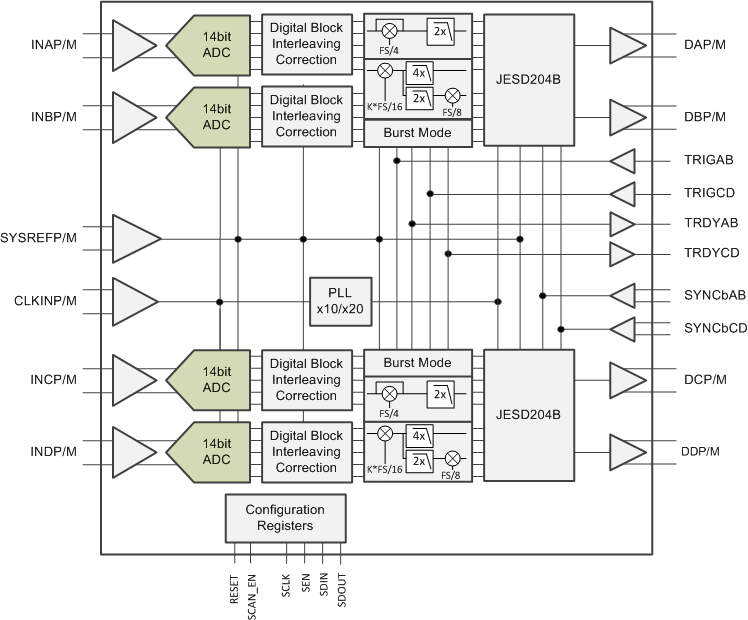
The ADS58J63 is a low power, wide bandwidth 14-bit 500 MSPS quad channel telecom receiver IC. It supports the JESD204B serial interface with data rates up to 10 Gbps supporting 1 lane per channel. The buffered analog input provides uniform input impedance across a wide frequency range while minimizing sample-and-hold glitch energy. The ADS58J63 provides excellent spurious-free dynamic range (SFDR) over a large input frequency range with very low power consumption. Its digital block includes a 2x and 4x decimation low pass filter with FS/4 and k×FS/16 mixers to support a receive bandwidth up to 200 MHz and a output burst mode for use as DPD observation receiver.
The JESD204B interface reduces the number of interface lines allowing high system integration density. An internal phase locked loop (PLL) multiplies the incoming ADC sampling clock to derive the bit clock which is used to serialize the 14bit data from each channel.
7.2 Functional Block Diagram
7.3 Feature Description
7.3.1 Analog Inputs
The ADS58J63 analog signal inputs are designed to be driven differentially. The analog input pins have internal analog buffers that drive the sampling circuit. As a result of the analog buffer, the input pins present a high impedance input across a very wide frequency range to the external driving source which enables great flexibility in the external analog filter design as well as excellent 50 Ω matching for RF applications. The buffer also helps to isolate the external driving circuit from the internal switching currents of the sampling circuit which results in a more constant SFDR performance across input frequencies.
The common-mode voltage of the signal inputs is internally biased to 1.9 V using 600-Ω resistors which allows for AC coupling of the input drive network. Each input pin (INP, INM) must swing symmetrically between (VCM + 0.475 V) and (VCM – 0.475 V), resulting in a 1.9-Vpp (default) differential input swing. The input sampling circuit has a 3-dB bandwidth that extends up to 900 MHz.
7.3.2 Recommended Input Circuitry
In order to achieve optimum AC performance the following circuitry is recommended at the analog inputs.
 Figure 51. Analog Input Driving Circuit
7.4 Device Functional Modes
7.4.1 Digital Features
The ADS58J63 supports decimation by 2 and 4 and burst mode output. The 4 channels can be configured as pairs (A and B and C and D) to either burst or decimation mode (must be same decimation mode for all 4 channels).
Table 1. Overview of Operating Modes
| OPERATING MODE |
DESCRIPTION | DIGITAL MIXER |
DECIMATION | BANDWIDTH AT 491Msps | BANDWIDTH AT 368Msps | OUTPUT FORMAT |
MAX OUTPUT RATE |
|---|---|---|---|---|---|---|---|
| 0 | Decimation | ±FS/4 | 2 | 200 MHz | 150 MHz | Complex | 250 Msps |
| 2 | – | 2 | 100 MHz | 75 MHz | Real | 250 Msps | |
| 4 | N×Fs/16 | 2 | 100 MHz | 75 MHz | Real | 250 Msps | |
| 5 | N×Fs/16 | 2 | 200 MHz | 150 MHz | Complex | 250 Msps | |
| 6 | N×Fs/16 | 4 | 100 MHz | 75 MHz | Complex | 125 Msps | |
| 7 | N×Fs/16 | 2 | 100 MHz | 75 MHz | Real | 500 Msps | |
| 8 | Burst Mode | – | – | 245.76 MHz | 184.32 MHz | Real | 500 Msps |
Figure 52 shows signal processing in Digital Down-Conversion (DDC) Block in ADS58J63.
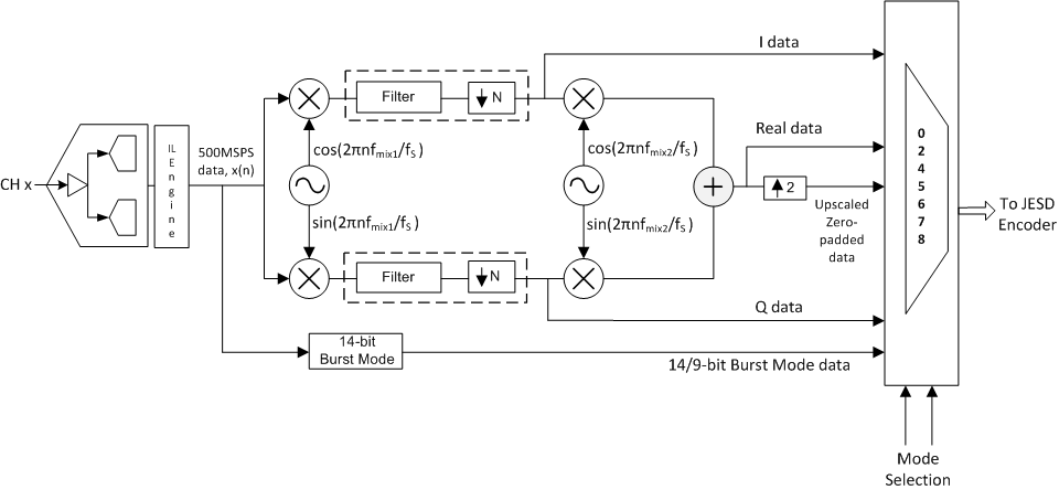 Figure 52. Digital Down-Conversion (DDC) Block
Table 2 shows characteristics of different blocks of DDC signal processing blocks active in different modes.
Table 2. Features of DDC Block in Different Modes
| Mode | fmix1 | Filter and Decimation | fmix 2 | Output |
|---|---|---|---|---|
| 0 | fS/4 | LPF cut off freq at fS/4, decimation by 2 | not used | I, Q data at 250 MSPS each is given out |
| 2 | not used | LPF or HPF cut off at fS/4, decimation by 2 | not used | Straight 250 MSPS data is given out |
| 4 | k fS/16 | LPF cutoff at fS/8, decimation by 2 | fS/8 | Real data at 250 MSPS is given out |
| 5 | k fS/16 | LPF cutoff at fS/8, decimation by 2 | not used | I, Q data at 250 MSPS each is given out |
| 6 | k fS/16 | LPF cutoff at fS/8, decimation by 4 | not used | I, Q data at 125 MSPS each is given out |
| 7 | k fS/16 | LPF cutoff at fS8, decimation by 2 | fS/8 | Real data is up-scaled, zero-padded and given out at 500 MSPS |
| 8 | not used | not used | not used | Straight 500 MSPS Burst mode data is given out |
7.4.2 Mode 0 – Decimation by 2 with IQ Outputs for up to 220 MHz of IQ Bandwidth
In this configuration, the DDC block includes a fixed frequency ±Fs/4 complex digital mixer preceding the digital filter – so the IQ passband is ± ~110 MHz (3 dB) centered at Fs/4. Mixing with +FS/4 inverts the spectrum. The stop band attenuation is approximately 90 dB and the passband flatness is ±0.1 dB. Figure 53 shows mixing operation in DDC Mode 0.
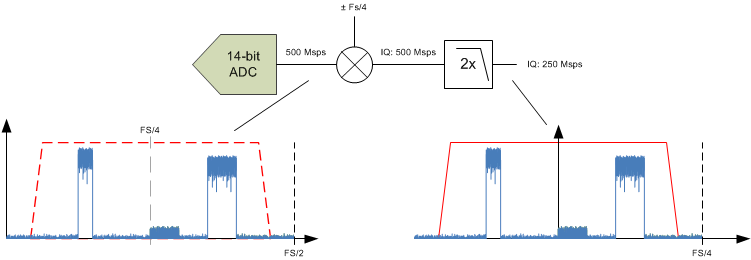 Figure 53. Mixing in Mode 0
Table 3. Filter Specification Details – Mode 0
| CORNERS | LOW PASS |
|---|---|
| –0.1 dB | 0.204 × Fs |
| –0.5 dB | 0.211 × Fs |
| –1 dB | 0.216 × Fs |
| –3 dB | 0.226 × Fs |
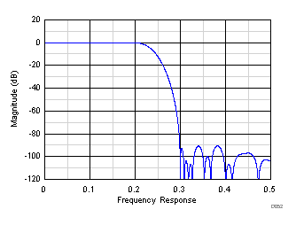 Figure 54. Frequency Response of Filter in Mode 0
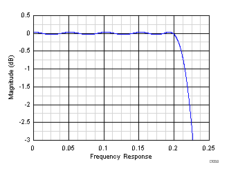 Figure 55. Zoomed view of Frequency Response
7.4.3 Mode 2 – Decimation by 2 for up to 110 MHz of Real Bandwidth
In this configuration, the DDC block only includes a 2x decimation filter (high pass or low pass) with real outputs. The passband is ~110 MHz (3 dB). Figure 56 shows filtering operation in DDC Mode 2.
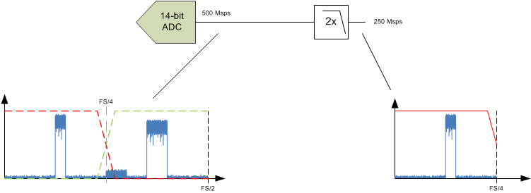 Figure 56. Filtering in Mode 2
Table 4. Filter Specification Details – Mode 2
| CORNERS | LOW PASS | HIGH PASS |
|---|---|---|
| –0.1 dB | 0.204 × Fs | 0.296 × Fs |
| –0.5 dB | 0.211 × Fs | 0.290 × Fs |
| –1 dB | 0.216 × Fs | 0.284 × Fs |
| –3 dB | 0.226 × Fs | 0.274 × Fs |
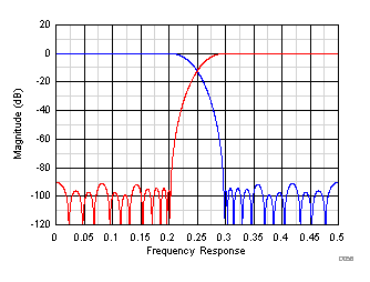 Figure 57. Frequency Response for Decimate-by-2 Low Pass and High Pass Filter (in Mode 2)
 Figure 58. Zoomed View of Frequency Response
7.4.4 Mode 4/7 – Decimation by 2 with Real Outputs for up to 110 MHz of Bandwidth
In this configuration, the DDC block includes a selectable N×Fs/16 complex digital mixer (N from –8 to +7) preceding the decimation by 2 digital filter also with an IQ passband of ± ~55 MHz (3 dB) centered at N×Fs/16. A positive value for N inverts the spectrum. In addition a Fs/8 complex digital mixer is added after the decimation filter transforming the output back to real format while centering the output spectrum within the Nyquist zone.
In addition the ADS58J63 supports a 0-pad feature where a sample with value = 0 gets added after each sample. In that way the output data rate gets interpolated to 500 Msps (real) with a 2nd image inverted at Fs/2-Fin.
The stop band attenuation is approximately 90 dB for in-band aliases from negative frequencies and ~55 dB for out of band aliases. The passband flatness is ±0.1 dB.
 Figure 59. Mixing and Filtering in Mode 4/7
Table 5. Filter Specification Details – Mode 4/7
| CORNERS | LOW PASS |
|---|---|
| –0.1 dB | 0.102 × Fs |
| –0.5 dB | 0.105 × Fs |
| –1 dB | 0.108 × Fs |
| –3 dB | 0.113 × Fs |
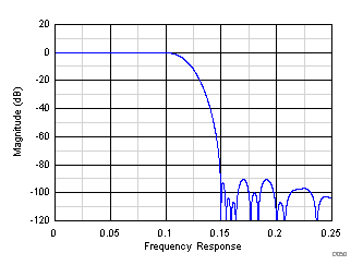 Figure 60. Frequency Response for Decimate-by-2 Low-Pass Filter (in Mode 4 and Mode 7)
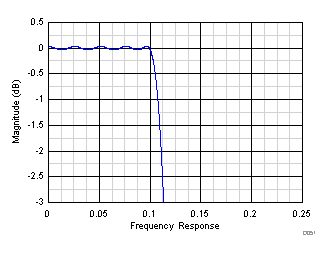 Figure 61. Zoomed View of Frequency Response
7.4.5 Mode 5 – Decimation by 2 with IQ Outputs for up to 110 MHz of IQ Bandwidth
In this configuration, the DDC block includes a selectable N×Fs/16 complex digital mixer (N from –8 to +7) preceding the decimation by 2 digital filter – so the IQ passband is ± ~55 MHz (3 dB) centered at N×Fs/16. A positive value for N inverts the spectrum.
The stop band attenuation is approximately 90 dB for in-band aliases from negative frequencies. The passband flatness is ±0.1 dB.
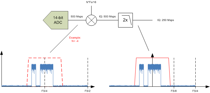 Figure 62. Mixing and Filtering in Mode 5
Table 6. Filter Specification Details – Mode 5
| CORNERS | LOW PASS |
|---|---|
| –0.1 dB | 0.102 × Fs |
| –0.5 dB | 0.105 × Fs |
| –1 dB | 0.108 × Fs |
| –3 dB | 0.113 × Fs |
 Figure 63. Frequency Response for Decimate-by-2 Low-Pass Filter (in Mode 5)
 Figure 64. Zoomed View of Frequency Response
7.4.6 Mode 6 – Decimation by 4 with IQ Outputs for up to 110 MHz of IQ Bandwidth
In this configuration, the DDC block includes a selectable n×Fs/16 complex digital mixer (n from –8 to +7) preceding the decimation by 4 digital filter – so the IQ passband is ± ~55 MHz (3 dB) centered at n×Fs/16. A positive value for N inverts the spectrum. The decimaiton by 4 filter is a cascade of two decimation by 2 filters with frequency response shown in Figure 66.
The stop band attenuation is approximately 90 dB for in-band aliases from negative frequencies and ~55 dB for out of band aliases. The passband flatness is ±0.1 dB.
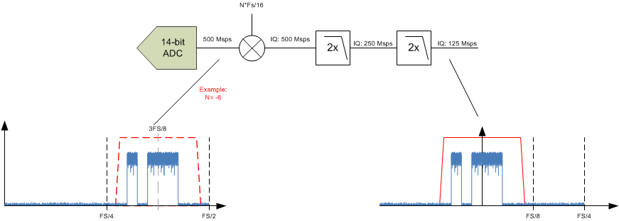 Figure 65. Mixing and Filtering in Mode 6
Table 7. Filter Specification Details – Mode 6
| CORNERS | LOW PASS |
|---|---|
| –0.1 dB | 0.102 × Fs |
| –0.5 dB | 0.105 × Fs |
| –1 dB | 0.108 × Fs |
| –3 dB | 0.113 × Fs |
 Figure 66. Frequency Response for Decimate-by-2 Low-Pass Filter (in Mode 6)
 Figure 67. Zoomed View of Frequency Response
7.4.7 Mode 8 – Burst Mode
In burst mode the output data is alternated between low resolution (L, 9-bit) and high resolution (H, 14-bit) output. The burst mode can be configured via SPI register writes independently for channel A/B and channel C/D.
The high resolution output is 14 bit and the number (#) of high and low resolution samples is set with two user programmable counters – one for high resolution (HC) and one for low resolution (LC). There is one counter pair (HC, LC) for channel A/B and one pair for channel C/D. The internal logic checks if the maximum duty cycle is exceeded and if necessary resets the counters to its default values.
Each output cycle starts with a low resolution and the counter values can be reconfigured for the next cycle during prior to the start of the next cycle.
 Figure 68. Timing Diagram for 14-bit Burst Mode (DDC Mode 8)
The counter values for high and low resolution can be programmed to:
High resolution counter (HC): 1 to 225
Low resolution counter (LC); 1 to 228
The output duty cycle limit is illustrated in Table 8.
Table 8. Output Duty Cycle Limit
| HIGH RESOLUTION OUTPUT | LOW RESOLUTION OUTPUT | MAXIMUM ALLOWED DUTY CYCLE (high : low resolution output) |
DEFAULT VALUE HC |
DEFAULT VALUE LC |
|---|---|---|---|---|
| 14 bit | 9 bit | 1/3 | 1 | 3 |
7.4.8 Trigger Input
The burst mode can be operated in auto trigger or manual trigger mode. In manual trigger mode the TRIGGER input (TRIGAB, TRIGCD) is used to release the high resolution data (HC) burst after the low resolution data counter LC has timed out. In auto trigger mode the high resolution data is released immediately after completion of the last low resolution sample.
Using SPI control the ADS58J63 can be configured to use TRIGAB or TRIGCD as the manual trigger input.
7.4.9 Manual Trigger Mode
Upon enabling manual trigger mode, the ADS58J63 starts transmission of low resolution data. As soon as the LC counter is finished, the manual trigger is unlocked, the trigger ready flag (TRDY) is raised and the high resolution output H can be triggered. Once the low resolution counter LC is finished, the next high resolution output or burst mode sequence can be triggered again. The HRES flag is embedded in the JESD204B output data stream. The counter values can be updated until a new burst mode cycles starts with transmission of low resolution samples.
Example of burst mode with manual trigger:
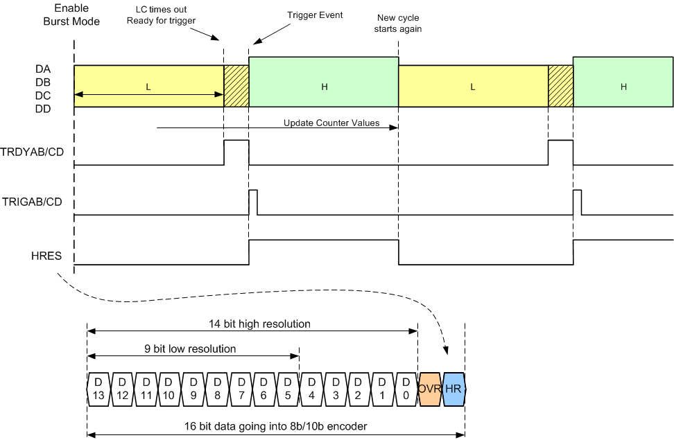 Figure 69. Timing Diagram for Manual Trigger Mode
7.4.10 Auto Trigger Mode
Upon enabling auto trigger mode, the ADS58J63 starts transmission of low resolution data. As soon as the low resolution samples counter (LC) is finished, the ADS58J63 immediately begins transmitting the high resolution output H. The HRES flag can also be embedded in the JESD204B output data stream. The counter values can be updated until a new burst mode cycles starts with transmission of low resolution samples. Any input on the trigger input pins is ignored.
Example of burst mode with automatic trigger:
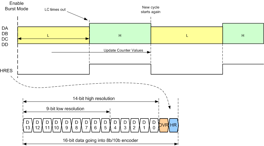 Figure 70. Timing Diagram for Auto Trigger Mode
7.4.11 Over-range Indication
The ADS58J63 provides a fast over-range indication (FOVR) which can be presented in the digital output data stream via SPI configuration. When the FOVR indication is embedded in the output data stream, it replaces the LSB (normal 0) of the 16 bit going to the 8b/10b encoder.
One threshold is set per channel pair A/B and C/D.
 Figure 71. Timing Diagram for FOVR
The fast OVR is triggered if the input voltage exceeds the programmable overrange threshold and it gets presented after just 44 input clock cycles enabling a quicker reaction to an overrange event.
The input voltage level at which the overload is detected is referred to as the threshold. It is programmable using the FOVR THRESHOLD bits.
The input voltage level at which fast OVR is triggered is:
Full-scale × [the decimal value of the FOVR Threshold bits] / 255)
The default threshold is E3h (227) which corresponds to a threshold of –1 dBFS.
In terms of full scale input, the fast OVR threshold can be calculated as shown in Equation 1:
Following is an example register write to set the FOVR threshold for all 4 channels:
Table 9. Register Sequence for FOVR Configuration
| ADDRESS | DATA | COMMENT |
|---|---|---|
| 11h | 80h | Go to Master page |
| 59h | 20h | Enable FOVR |
| 11h | FFh | Go to ADC page |
| 5Fh | FFh | Set FOVR threshold for chCD to 255 |
| 4004h | 68h | Go to main digital page |
| 4003h | 00h | |
| 60ABh | 01h | Enable bit D0 overwrite |
| 60ADh | 03h | Select FOVR to replace bit D0 |
| 6000h | 01h | Issue and clear digital reset |
| 6000h | 00h |
7.4.12 Power-Down Mode
The ADS58J63 provides a highly-configurable power-down mode. Power-down can be enabled using the PDN pin or SPI register writes.
A power-down mask can be configured, which allows a trade-off between wake-up time and power consumption in power-down mode. Two independent power-down masks can be configured: MASK 1 and MASK 2 as shown in Table 10. See the master page registers in Table 15 for further details.
Table 10. Register Address for Power-Down Modes
| REGISTER ADDRESS | COMMENT | REGISTER DATA | |||||||
|---|---|---|---|---|---|---|---|---|---|
| A[7:0] (Hex) | 7 | 6 | 5 | 4 | 3 | 2 | 1 | 0 | |
| MASTER PAGE (80h) | |||||||||
| 20 | MASK 1 | PDN ADC CHAB | PDN ADC CHCD | ||||||
| 21 | PDN BUFFER CHCD | PDN BUFFER CHAB | 0 | 0 | 0 | 0 | |||
| 23 | MASK 2 | PDN ADC CHAB | PDN ADC CHCD | ||||||
| 24 | PDN BUFFER CHCD | PDN BUFFER CHAB | 0 | 0 | 0 | 0 | |||
| 26 | CONFIG | GLOBAL PDN | OVERRIDE PDN PIN | PDN MASK SEL | 0 | 0 | 0 | 0 | 0 |
| 53 | 0 | MASK SYSREF | 0 | 0 | 0 | 0 | 0 | 0 | |
| 55 | 0 | 0 | 0 | PDN MASK | 0 | 0 | 0 | 0 | |
To save power, the device can be put in complete power down by using the GLOBAL PDN register bit. However, when JESD link must remain up while putting the device in power down, the ADC and analog buffer can be powered down by using the PDN ADC CHx and PDN BUFFER CHx register bits after enabling the PDN MASK register bit. The PDN MASK SEL register bit can be used to select between MASK 1 or MASK 2. Table 11 shows power consumption for different combinations of the GLOBAL PDN, PDN ADC CHx, and PDN BUFF CHx register bits.
Table 11. Power Consumption in Different Power-Down Settings
| REGISTER BIT | COMMENT | IAVDD3V (mA) | IAVDD (mA) | IDVDD (mA) | IIOVDD (mA) | TOTAL POWER (W) |
|---|---|---|---|---|---|---|
| Default | After reset, with a full-scale input signal to both channels | 0.340 | 0.365 | 0.184 | 0.533 | 2.675 |
| GBL PDN = 1 | The device is in complete power-down state | 0.002 | 0.006 | 0.012 | 0.181 | 0.247 |
| GBL PDN = 0, PDN ADC CHx = 1 (x = AB or CD) |
The ADCs of one pair of channels are powered down | 0.277 | 0.225 | 0.123 | 0.496 | 2.063 |
| GBL PDN = 0, PDN BUFF CHx = 1 (x = AB or CD) |
The input buffers of one pair of channels iarepowered down | 0.266 | 0.361 | 0.187 | 0.527 | 2.445 |
| GBL PDN = 0, PDN ADC CHx = 1, PDN BUFF CHx = 1 (x = AB or CD) |
The ADCs and input buffers of one pair of channels are powered down | 0.200 | 0.224 | 0.126 | 0.492 | 1.830 |
| GBL PDN = 0, PDN ADC CHx = 1, PDN BUFF CHx = 1 (x = AB and CD) |
The ADCs and input buffers of all channels are powered down | 0.060 | 0.080 | 0.060 | 0.448 | 0.960 |
7.5 Programming
7.5.1 Device Configuration
The ADS58J63 can be configured using a serial programming interface, as described below. In addition, the device has one dedicated parallel pin (PDN) for controlling the power down modes. The ADS58J63 supports a 24-bit (16-bit address, 8-bit data) SPI operation and uses paging (see detailed register map info) to access all register bits.
7.5.1.1 Details of Serial Interface
The ADC has a set of internal registers that can be accessed by the serial interface formed by the SEN (serial interface enable), SCLK (serial interface clock) and SDIN (serial interface data) pins. Serial shift of bits into the device is enabled when SEN is low. Serial data on SDIN are latched at every SCLK rising edge when SEN is active (low). The interface can work with SCLK frequencies from 5 MHz down to very low speeds (of a few hertz) and also with non-50% SCLK duty cycle.
 Figure 72. Serial Interface Timing Diagram
Table 12. Programing Details of Serial Interface
| SPI BITS | DESCRIPTION | OPTIONS |
|---|---|---|
| R/W | Read/write bit | 0 = SPI write 1 = SPI read back |
| M | SPI bank access | 0 = Analog SPI bank (Master and ADC page) 1 = JDigital SPI bank (Main Digital, Analog JESD, and Digital JESD pages) |
| P | JESD page selection bit | 0 = Page access 1 = Register access |
| CH | SPI access for a specific channel of the digital SPI bank | 0 = Channel AB 1 = Channel CD By default, both channels are being addressed. |
| ADDR [11:0] | SPI address bits | — |
| DATA [7:0] | SPI data bits | — |
7.5.1.2 Serial Register Write: Analog Bank
The analog SPI bank contains of two pages (the master and ADC page). The internal register of the ADS58J63 analog SPI bank can be programmed by:
- Drive the SEN pin low.
- Initiate a serial interface cycle specifying the page address of the register whose content must be written.
- Master page: write address 0011h with 80h.
- ADC page: write address 0011h with 0Fh.
- Write the register content as shown in Figure 73. When a page is selected, multiple writes into the same page can be done.
 Figure 73. Serial Register Write Timing Diagram
7.5.1.3 Serial Register Readout: Analog Bank
The content from one of the two analog banks can be read out by:
- Drive the SEN pin low.
- Select the page address of the register whose content must be read.
- Master page: write address 0011h with 80h.
- ADC page: write address 0011h with 0Fh.
- Set the R/W bit to 1 and write the address to be read back.
- Read back the register content on the SDOUT pin, as shown in Figure 74. When a page is selected, multiple read backs from the same page can be done.
 Figure 74. Serial Register Read Timing Diagram
7.5.1.4 JESD Bank SPI Page Selection
The JESD SPI bank contains four pages (main digital, interleaving engine, digital, and analog JESD pages). The individual pages can be selected by:
- Drive the SEN pin low.
- Set the M bit to 1 and specify the page with two register writes. Note that the P bit must be set to 0, as shown in Figure 75.
- Write address 4003h with 00h (LSB byte of page address).
- Write address 4004h with the MSB byte of the page address.
- For Main digital page: write address 4004h with 68h.
- For Digital JESD page: write address 4004h with 69h.
- For Analog JESD page: write address 4004h with 6Ah.
- For Interleaving engine page: write address 4004h with 61h.
 Figure 75. SPI Page Selection
7.5.1.5 Serial Register Write: Analog Bank
The analog SPI bank contains two pages (Master and ADC page). The internal register of the ADS58J63 analog SPI bank can be programmed following these steps:
- Drive the SEN pin low.
- Initiate a serial interface cycle specifying the page address of the register whose content has to be written
- Master page: write address 11h with 80h
- ADC page: write address 11h with 0Fh
- Write register content. Once a page is selected, multiple writes into the same page can be done.
 Figure 76. Serial Register Write Timing Diagram
7.5.1.6 Serial Register Readout: Analog Bank
SPI read out of content in one of the two analog banks can be accomplished with the following steps:
- Drive the SEN pin low.
- Select the page address of the register which content has to be read.
- Master page: write Address = 11h with 80h
- ADC page: write Address 11h with 0Fh.
- Set the R/W bit to '1' and write the address to be read back.
- Read back register content on the SDOUT pin. Once a page is selected, multiple read backs from the same page can be done.
 Figure 77. Serial Register Read Timing Diagram
7.5.1.7 Digital Bank SPI Page Selection
The Digital SPI bank contains five pages (Main digital, Interleaving Engine, Decimation filter, JESD digital, and JESD analog). The individual pages can be selected following these steps:
- Drive the SEN pin low.
- Set the M bit to ‘1’ and specify the page with two register writes (Note: P bit set to 0)
- Write address 4003h with 00h (LSB byte of page address)
- Write address 4004h MSB byte of page address
- Main digital page: write Address = 4004h with 68h (default)
- Digital JESD page: write Address = 4004h with 69h
- Analog JESD page: write Address = 4004h with 6Ah
- Interleaving Engine page: write Address = 4004h with 61h
- Decimation Filter page: write Address = 4004h with 61h and 4003h with 41h
spacer
 Figure 78. SPI Timing Diagram for Digital Bank Page Selection
7.5.1.8 Serial Register Write – Digital Bank
The ADS58J63 is a quad channel device and the JESD204B portion is configured individually for 2 channel (A/B and C/D) using the CH bit. Note the P bit needs to be set to 1 for register writes.
- Drive the SEN pin low.
- Select the digital bank page (Note: M bit = 1, P bit = 0)
- Write address 4003h with 00h
- Main digital page: write Address = 4004h with 68h (default)
- Digital JESD page: write Address = 4004h with 69h
- Analog JESD page: write Address = 4004h with 6Ah
- Interleaving Engine page: write Address = 4004h with 61h
- Decimation Filter page: write Address = 4004h with 61h and 4003h with 41h
- Set M and P bit to 1 and select ChAB (CH=0) or ChCD (CH=1) and write register content. Once a page is selected, multiple writes into the same page can be done.
By default, register writes are applied to both channel pairs (broadcast mode). To disable broadcast mode and enable individual channel writes, write address 4005h with 01h (default is 00h).
 Figure 79. Serial Register Write Timing Diagram
7.5.1.9 Individual Channel Programming
By default, register writes are applied to both channels. To enable individual channel writes, write address 4005h with 01h (default is 00h).
7.5.1.10 Serial Register Readout – Digital Bank
SPI read out of content in one of the three digital banks can be accomplished with the following steps:
- Drive the SEN pin low.
- Select the digital bank page (Note: M bit = 1, P bit = 0)
- Write address 4003h with 00h
- Main digital page: write Address = 4004h with 68h
- Digital JESD page: write Address = 4004h with 69h
- Analog JESD page: write Address = 4004h with 6Ah
- Interleaving Engine page: write Address = 4004h with 61h
- Decimation Filter page: write Address = 4004h with 61h and 4003h with 41h
- Set the R/W bit, M and P bit to '1' and select ChAB) or ChCD and write the address to be read back.
- Read back register content on the SDOUT pin. Once a page is selected, multiple read backs from the same page can be done.
 Figure 80. Serial Register Read Timing Diagram
7.5.2 JESD204B Interface
The ADS58J63 supports device subclass 1 with a maximum output data rate of 10 Gbps for each serial transmitter.
An external SYSREF signal is used to align all internal clock phases and the local multi frame clock to a specific sampling clock edge. This allows synchronization of multiple devices in a system and minimizes timing and alignment uncertainty. The ADS58J63 supports single (for all 4 JESD links) or dual (for channel A/B and C/D) SYNCb inputs and can be configured via SPI.
 Figure 81. JESD Interface Block Diagram
Depending on the ADC sampling rate, the JESD204B output interface can be operated with 1 lane per channel. The JESD204B setup and configuration of the frame assembly parameters is handled via SPI interface.
The JESD204B transmitter block consists of the transport layer, the data scrambler and the link layer. The transport layer maps the ADC output data into the selected JESD204B frame data format and manages if the ADC output data or test patterns are being transmitted. The link layer performs the 8b/10b data encoding as well as the synchronization and initial lane alignment using the SYNC input signal. Optionally data from the transport layer can be scrambled.
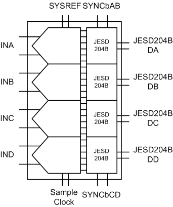 Figure 82. JESD204B Transmitter Block
7.5.2.1 JESD204B Initial Lane Alignment (ILA)
The initial lane alignment process is started by the receiving device by de-asserting the SYNCb signal. Upon detecting a logic low on the SYNC input pins, the ADS58J63 starts transmitting comma (K28.5) characters to establish code group synchronization.
Once synchronization is completed the receiving device re-asserts the SYNCb signal and the ADS58J63 starts the initial lane alignment sequence with the next local multi frame clock boundary. The ADS58J63 transmits 4 multi-frames each containing K frames (K is SPI programmable). Each of the multi-frames contains the frame start and end symbols and the 2nd multi-frame also contains the JESD204 link configuration data.
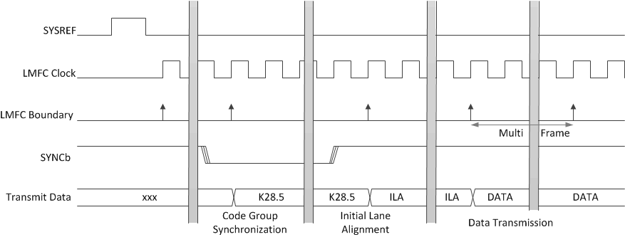 Figure 83. ILA Sequence
7.5.2.2 JESD204B Frame Assembly
The JESD204B standard defines the following parameters:
- L is the number of lanes per link.
- M is the number of converters per device.
- F is the number of octets per frame clock period.
- S is the number of samples per frame.
Table 13 lists the available JESD204B formats and valid ranges for the ADS58J63. The ranges are limited by the Serdes line rate and the maximum ADC sample frequency.
Table 13. Available JESD204B Formats and Valid Ranges for the ADS58J63
| L | M | F | S | OPERATING MODE | DIGITAL MODE | OUTPUT FORMAT | JESD MODE (69h, 01h) |
JESD PLL MODE (6Ah, 01h6) |
MAX ADC OUTPUT RATE (Msps) |
MAX fSERDES
(Gbps) |
|---|---|---|---|---|---|---|---|---|---|---|
| 4 | 8 | 4 | 1 | 0,5 | 2x Decimation | Complex | 40 x | 40 x | 250 | 10.0 |
| 4 | 4 | 2 | 1 | 2,4 | 2x Decimation | Real | 20 x | 20 x | 250 | 5.0 |
| 2 | 4 | 4 | 1 | 2,4 | 2x Decimation | Real | 40 x | 40 x | 250 | 10.0 |
| 4 | 8 | 4 | 1 | 6 | 4x Decimation | Complex | 40 x | 20 x | 125 | 5.0 |
| 2 | 8 | 8 | 1 | 6 | 4x Decimation | Complex | 80 x | 40 x | 125 | 10.0 |
| 4 | 4 | 2 | 1 | 7 | 2x Decimation with ‘0-Pad’ | Real | 20 x | 40 x | 500 | 10.0 |
| 4 | 4 | 2 | 1 | 8 | Burst Mode | Real | 20 x | 40 x | 500 | 10.0 |
The detailed frame assembly is shown in Table 14.
Table 14. Detailed Frame Assembly
| LMFS = 4841 | LMFS = 4421 | LMFS = 4421 (0-Pad) | ||||||||||||
|---|---|---|---|---|---|---|---|---|---|---|---|---|---|---|
| DA | AI0[15:8] | AI0[7:0] | AQ0[15:8] | AQ0[7:0] | A0[15:8] | A0[7:0] | A1[15:8] | A1[7:0] | A0[15:8] | A0[7:0] | 0000 0000 | 0000 0000 | ||
| DB | BI0[15:8] | BI0[7:0] | BQ0[15:8] | BQ0[7:0] | B0[15:8] | B0[7:0] | B1[15:8] | B1[7:0] | B0[15:8] | B0[7:0] | 0000 0000 | 0000 0000 | ||
| DC | CI0[15:8] | CI0[7:0] | CQ0[15:8] | CQ0[7:0] | C0[15:8] | C0[7:0] | C1[15:8] | C1[7:0] | C0[15:8] | C0[7:0] | 0000 0000 | 0000 0000 | ||
| DD | DI0[15:8] | DI0[7:0] | DQ0[15:8] | DQ0[7:0] | D0[15:8] | D0[7:0] | D1[15:8] | D1[7:0] | D0[15:8] | D0[7:0] | 0000 0000 | 0000 0000 | ||
| LMFS = 2441 | LMFS = 2881 | ||||||||||||
| DB | A0[15:8] | A0[7:0] | B0[15:8] | B0[7:0] | AI0[15:8] | AI0[7:0] | AQ0[15:8] | AQ0[7:0] | BI0[15:8] | BI0[7:0] | BQ0[15:8] | BQ0[7:0] | |
| DC | C0[15:8] | C0[7:0] | D0[15:8] | D0[7:0] | CI0[15:8] | CI0[7:0] | CQ0[15:8] | CQ0[7:0] | DI0[15:8] | DI0[7:0] | DQ0[15:8] | DQ0[7:0] | |
7.5.2.3 JESD Output Switch
The ADS58J63 provides a digital cross point switch in the JESD204B block which allows internal routing of any output of the 2 ADCs within one channel pair to any of the 2 JESD204B serial transmitters in order to ease layout constraints. The cross point switch routing is configured via SPI (address 21h in JESD digital page).
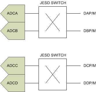 Figure 84. Switching the Output Lanes
7.5.2.3.1 Serdes Transmitter Interface
Each of the 10 Gbps serdes transmitter outputs requires AC coupling between transmitter and receiver. The differential pair should be terminated with 100 Ω as close to the receiving device as possible to avoid unwanted reflections and signal degradation.
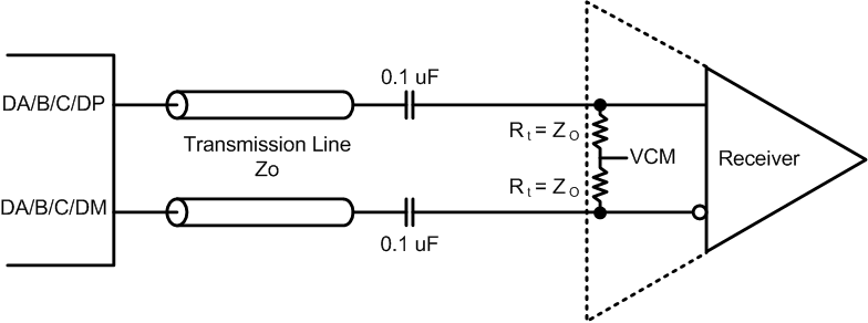 Figure 85. Serdes Transmitter Connection to Receiver
7.5.2.3.2 SYNCb Interface
The ADS58J63 supports single (either SYNCb input controls all 4 JESD204B links) or dual (1 SYNCb input controls 2 JESD204B lanes (DA/DB and DC/DD) SYNCb control. When using single SYNCb control, the unused input should be connected to differential logic low (SYNCbxxP = 0 V, SYNCbxxM = IOVDD).
7.5.2.3.3 Eye Diagram
Figure 86 to Figure 89 show the serial output eye diagrams of the ADS58J63 at 5 Gbps and 10 Gbps with default and increased output voltage swing against the JESD204B mask.
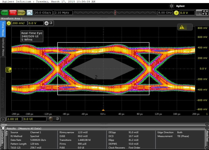 Figure 86. Eye at 5-Gbps Bit Rate with
 Default Output Swing
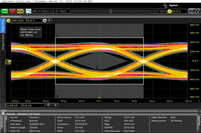 Figure 88. Eye at 10-Gbps Bit Rate with
 Default Output Swing
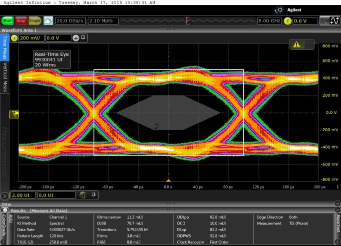 Figure 87. Eye at 5-Gbps Bit Rate with
 Increased Output Swing
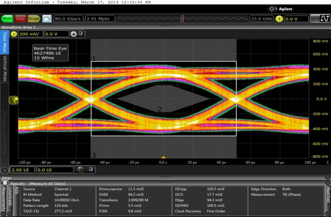 Figure 89. Eye at 10-Gbps Bit Rate with
 Increased Output Swing
7.6 Register Maps
The conceptual diagram of Serial Registers is shown in Figure 90.
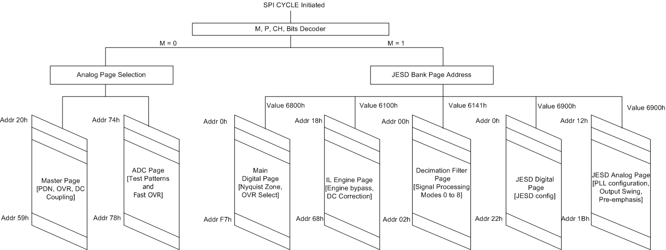 Figure 90. Serial Interface Registers
7.6.1 Detailed Register Info
The ADS58J63 contains two main SPI banks. The analog SPI bank gives access to the ADC cores while the digital SPI bank controls the serial interface. The analog SPI bank is divided into two pages (MASTER and ADC) while the digital SPI bank is divided into five pages (Main digital, Interleaving Engine, Decimation filter, JESD digital, and JESD analog).
Table 15. Register Map
| Register Address | Register Data | |||||||
|---|---|---|---|---|---|---|---|---|
| A7-A0 in hex | D7 | D6 | D5 | D4 | D3 | D2 | D1 | D0 |
| 0 | RESET | 0 | 0 | 0 | 0 | 0 | 0 | RESET |
| 3 | JESD BANK PAGE SEL [7:0] | |||||||
| 4 | JESD BANK PAGE SEL [15:8] | |||||||
| 5 | 0 | 0 | 0 | 0 | 0 | 0 | 0 | DIS BROADCAST |
| 11 | ANALOG PAGE SELECTION [7:0] | |||||||
| MASTER PAGE (80h) | ||||||||
| 20 | PDN ADC CHAB | PDN ADC CHCD | ||||||
| 21 | PDN BUFFER CHCD | PDN BUFFER CHAB | 0 | 0 | 0 | 0 | ||
| 23 | PDN ADC CHAB | PDN ADC CHCD | ||||||
| 24 | PDN BUFFER CHCD | PDN BUFFER CHAB | 0 | 0 | 0 | 0 | ||
| 26 | GLOBAL PDN | OVERRIDE PDN PIN | PDN MASK SEL | 0 | 0 | 0 | 0 | 0 |
| 3A | 0 | BUFFER CURR INCREASE | 0 | 0 | 0 | 0 | 0 | 0 |
| 39 | ALWAYS WRITE 1 | 0 | 0 | 0 | 0 | 0 | 0 | |
| 53 | CLK DIV | MASK SYSREF | 0 | 0 | 0 | 0 | 0 | 0 |
| 55 | 0 | 0 | 0 | PDN MASK | 0 | 0 | 0 | 0 |
| 56 | 0 | 0 | 0 | 0 | INPUT BUFF CURR EN | 0 | 0 | 0 |
| 59 | 0 | 0 | ALWAYS WRITE 1 | 0 | 0 | 0 | 0 | 0 |
| ADC PAGE (0Fh) | ||||||||
| 5F | FOVR CHCD THRESH | |||||||
| 60 | 0 | 0 | 0 | PULSE BIT CHC | 0 | 0 | 0 | 0 |
| 61 | 0 | 0 | 0 | HD3 NYQ2 CHCD | 0 | 0 | 0 | PULSE BIT CHD |
| 6C | 0 | 0 | 0 | PULSE_BIT_CHA | 0 | 0 | 0 | 0 |
| 6D | 0 | 0 | 0 | HD3_NYQ2_CHAB | 0 | 0 | 0 | PULSE BIT CHB |
| 74 | TEST PATTERN ON CHANNEL | 0 | 0 | 0 | 0 | |||
| 75 | CUSTOM PATTERN 1 [13:6] | |||||||
| 76 | CUSTOM PATTERN 1 [5:0] | 0 | 0 | |||||
| 77 | CUSTOM PATTERN 2 [13:6] | |||||||
| 78 | CUSTOM PATTERN 2 [5:0] | 0 | 0 | |||||
| INTERLEAVING ENGINE PAGE (6100h) | ||||||||
| 18 | 0 | 0 | 0 | 0 | 0 | 0 | IL BYPASS | |
| 68 | 0 | 0 | 0 | 0 | 0 | DC CORR DIS | 0 | |
| DECIMATION FILTER PAGE (6141h) | ||||||||
| 0 | CHB/C FINE MIX | DDC MODE | ||||||
| 1 | 0 | 0 | 0 | 0 | DDC MODE6 EN1 | ALWAYS WRITE 1 | CHB/C HPF EN | CHB/C COARSE MIX |
| 2 | 0 | 0 | CHA/D HPF EN | CHA/D COARSE MIX | CHA/D FINE MIX | |||
| MAIN DIGITAL PAGE (6800h) | ||||||||
| 0 | 0 | 0 | 0 | 0 | 0 | 0 | 0 | IL RESET |
| 42 | 0 | 0 | 0 | 0 | 0 | NYQUIST ZONE | ||
| 4E | CTRL NYQUIST ZONE | 0 | 0 | 0 | 0 | 0 | 0 | 0 |
| AB | 0 | 0 | 0 | 0 | 0 | 0 | 0 | OVR EN |
| AD | 0 | 0 | 0 | 0 | OVR ON LSB | |||
| F7 | 0 | 0 | 0 | 0 | 0 | 0 | 0 | DIG RESET |
| JESD DIGITAL PAGE (6900h) | ||||||||
| 0 | CTRL K | JESD MODE EN | DDC MODE6 EN2 | TESTMODE EN | 0 | LANE ALIGN | FRAME ALIGN | TX LINK DIS |
| 1 | SYNC REG | SYNC REG EN | SYNCB SEL AB/CD | 0 | DDC MODE6 EN3 | 0 | JESD MODE | |
| 2 | LINK LAYER TESTMODE | LINK LAYER RPAT | LMFC MASK RESET | 0 | 0 | 0 | ||
| 3 | FORCE LMFC COUNT | LMFC COUNT INIT | RELEASE ILANE SEQ | |||||
| 5 | SCRAMBLE EN | 0 | 0 | 0 | 0 | 0 | 0 | 0 |
| 6 | 0 | 0 | 0 | FRAMES PER MULTI FRAME (K) | ||||
| 17 | HIRES FLAG ON LSB | 0 | TRIG SET AB/CD | AUTO TRIG EN | 0 | RATIO INVALID | 0 | |
| 19 | 0 | 0 | 0 | 0 | LC [27:24] | |||
| 1A | LC [23:16] | |||||||
| 1B | LC [15:8] | |||||||
| 1C | LC [7:0] | |||||||
| 1D | 0 | 0 | 0 | 0 | HC [27:24] | |||
| 1E | HC [23:16] | |||||||
| 1F | HC [15:8] | |||||||
| 20 | HC [7:0] | |||||||
| 21 | OUPUT CHA MUX SEL | OUTPUT CHB MUX SEL | OUTPUT CHC MUX SEL | OUTPUT CHD MUX SEL | ||||
| 22 | 0 | 0 | 0 | 0 | OUT CHA INV | OUT CHB INV | OUT CHC INV | OUT CHD INV |
| JESD ANALOG PAGE (6A00h) | ||||||||
| 12 | SEL EMP LANE A/D | 0 | 0 | |||||
| 13 | SEL EMP LANE B/C | 0 | 0 | |||||
| 16 | 0 | 0 | 0 | 0 | 0 | 0 | JESD PLL MODE | |
| 1B | JESD SWING | 0 | 0 | 0 | 0 | 0 | ||
7.6.2 Example Register Writes
Global Power Down
| ADDRESS | DATA | COMMENT |
|---|---|---|
| 11h | 80h | Set Master Page |
| 00h26 | 80h | Set Global Power Down |
Change decimation mode 0 (default) to mode 4 adjusting both the LMFS configuration (LMFS = 4841 to 4421) as well as serial output data rate (10 Gbps to 5 Gbps).
| ADDRESS | DATA | COMMENT |
|---|---|---|
| 4004h | 69h | Select digital JESD page |
| 4003h | 00h | |
| 6000h | 40h | Enables JESD mode overwrite |
| 6001h | 01h | Select digital to 20x mode |
| 4004h | 6Ah | Select analog JESD page |
| 6016h | 00h | Set serdes PLL to 20x mode |
| 4004h | 61h | Select decimation filter page |
| 4003h | 41h | |
| 6000h | CCh | Select mode 4 Digital mixer for chAB set to –4 (FS/4) |
| 6002h | 0Ch | Digital mixer for chCD set to –4 (FS/4) |
7.6.3 Register Descriptions
7.6.3.1 Register 0h (offset = 0h) [reset = 0h]
| A7-A0 in Hex | 7 | 6 | 5 | 4 | 3 | 2 | 1 | 0 |
|---|---|---|---|---|---|---|---|---|
| 0 | RESET | 0 | 0 | 0 | 0 | 0 | 0 | RESET |
| LEGEND: W = Write only; -n = value after reset |
Table 16. Register 0h Field Description
| Bit(1) | Name | Type | Reset | Description |
|---|---|---|---|---|
| D7 | RESET | R/W | 0 | 0 = Normal operation 1 = Internal software reset, clears back to 0 |
| D0 | RESET | R/W | 0 | 0 = Normal operation 1 = Internal software reset, clears back to 0 |
7.6.3.2 Register 3h/4h (offset = 3h/4h) [reset = 0h]
| A7-A0 in Hex | 7 | 6 | 5 | 4 | 3 | 2 | 1 | 0 |
|---|---|---|---|---|---|---|---|---|
| 3 | JESD BANK PAGE SEL [7:0] | |||||||
| 4 | JESD BANK PAGE SEL [16:8] | |||||||
| LEGEND: W = Write only; -n = value after reset |
Table 17. Register 3h/4h Field Description
| Bit | Name | Type | Reset | Description |
|---|---|---|---|---|
| D7 - D0 | JESD BANK PAGE SEL | R/W | 0 | Program these bits to access desired page in JESD Bank 6100h = Interleaving Engine Page selected 6141h = Decimation Filter Page Selected 6800h = Main Digital Page Selected 6900h = JESD Digtial Page selected 6A00h = JESD Analog Page selected |
7.6.3.3 Register 5h (offset = 5h) [reset = 0h]
| A7-A0 in Hex | 7 | 6 | 5 | 4 | 3 | 2 | 1 | 0 |
|---|---|---|---|---|---|---|---|---|
| 5 | 0 | 0 | 0 | 0 | 0 | 0 | 0 | DIS BROADCAST |
| LEGEND: W = Write only; -n = value after reset |
Table 18. Register 5h Field Description
| Bit | Name | Type | Reset | Description |
|---|---|---|---|---|
| D0 | DIS BROADCAST | R/W | 0 | 0 = Normal operation. Channel A and B are programmed as a pair. Channel C and D are programmed as a pair. 1 = channel A and B can be individually programmed based on bit 'CH'. Similarly channel C and D can be individually programmed based on bit 'CH'. |
7.6.3.4 Register 11h (offset = 11h) [reset = 0h]
| A7-A0 in Hex | 7 | 6 | 5 | 4 | 3 | 2 | 1 | 0 |
|---|---|---|---|---|---|---|---|---|
| 11 | ANALOG PAGE SELECTION [7:0] | |||||||
| LEGEND: R/W = Read/Write; -n = value after reset |
Table 19. Register 11h Field Descriptions
| Bit | Name | Type | Reset | Description |
|---|---|---|---|---|
| D7-D0 | ANALOG PAGE SELECTION [7:0] | R/W | 0 | Register page (only one page at a time can be addressed). Master page = 80h ADC page = 0Fh The 5 digital pages (Main digital, Interleaving Engine, Analog JESD, Digital JESD, and Decimation filter) are selected via the M bit. See Serial Interface Read/Write section for more details. |
7.6.3.5 Master Page (80h)
7.6.3.5.1 Register 20h (address = 20h) [reset = 0h] , Master Page (080h)
| A7-A0 in Hex | 7 | 6 | 5 | 4 | 3 | 2 | 1 | 0 |
| PDN ADC CHAB | PDN ADC CHCD | |||||||
| R/W-0h | R/W-0h | |||||||
| LEGEND: R/W = Read/Write; -n = value after reset |
Table 20. Registers 20h Field Descriptions
| Bit | Field | Type | Reset | Description |
|---|---|---|---|---|
| 7-4 | PDN ADC CHAB | R/W | 0h | There are two power-down masks that are controlled via the PDN mask register bit in address 55h. The power-down mask 1 or mask 2 are selected via register bit 5 in address 26h. Power-down mask 1: addresses 20h and 21h. Power-down mask 2: addresses 23h and 24h. See Power-Down Mode for details. |
| 3-0 | PDN ADC CHCD | R/W | 0h |
7.6.3.5.2 Register 21h (address = 21h) [reset = 0h] , Master Page (080h)
| A7-A0 in Hex | 7 | 6 | 5 | 4 | 3 | 2 | 1 | 0 |
| PDN BUFFER CHCD | PDN BUFFER CHAB | 0 | 0 | 0 | 0 | |||
| R/W-0h | R/W-0h | W-0h | R/W-0h | R/W-0h | W-0h | |||
| LEGEND: R/W = Read/Write; W = Write only; -n = value after reset |
Table 21. Register 21h Field Descriptions
| Bit | Field | Type | Reset | Description |
|---|---|---|---|---|
| 7-6 | PDN BUFFER CHCD | R/W | 0h | There are two power-down masks that are controlled via the PDN mask register bit in address 55h. The power-down mask 1 or mask 2 are selected via register address 26h, bit 5. Power-down mask 1: addresses 20h and 21h. Power-down mask 2: addresses 23h and 24h. See Power-Down Mode for details. |
| 5-4 | PDN BUFFER CHAB | R/W | 0h | |
| 3 | 0 | W | 0h | |
| 2-0 | 0 | W | 0h | Must write 0. |
7.6.3.5.3 Register 23h (address = 23h), Master Page (080h)
| A7-A0 in Hex | 7 | 6 | 5 | 4 | 3 | 2 | 1 | 0 |
| PDN BUFFER CHAB | PDN BUFFER CHCD | |||||||
| R/W-0h | R/W-0h | W-0h | R/W-0h | R/W-0h | W-0h | |||
| LEGEND: R/W = Read/Write; -n = value after reset |
Table 22. Register 23h Field Descriptions
| Bit | Field | Type | Reset | Description |
|---|---|---|---|---|
| 7-4 | PDN ADC CHAB | R/W | 0h | There are two power-down masks that are controlled via the PDN mask register bit in address 55h. The power-down mask 1 or mask 2 are selected via register bit 5 in address 26h. Power-down mask 1: addresses 20h and 21h. Power-down mask 2: addresses 23h and 24h. See Power-Down Mode for details. |
| 3-0 | PDN ADC CHCD | R/W | 0h |
7.6.3.5.4 Register 24h (address = 24h) [reset = 0h] , Master Page (080h)
| A7-A0 in Hex | 7 | 6 | 5 | 4 | 3 | 2 | 1 | 0 |
| PDN BUFFER CHCD | PDN BUFFER CHAB | 0 | 0 | 0 | 0 | |||
| R/W-0h | R/W-0h | W-0h | R/W-0h | R/W-0h | R/W-0h | |||
| LEGEND: R/W = Read/Write; W = Write only; -n = value after reset |
Table 23. Register 24h Field Descriptions
| Bit | Field | Type | Reset | Description |
|---|---|---|---|---|
| 7-6 | PDN BUFFER CHCD | R/W | 0h | There are two power-down masks that are controlled via the PDN mask register bit in address 55h. The power-down mask 1 or mask 2 are selected via register address 26h, bit 5. Power-down mask 1: addresses 20h and 21h. Power-down mask 2: addresses 23h and 24h. See Power-Down Mode for details. |
| 5-4 | PDN BUFFER CHAB | R/W | 0h | |
| 3 | 0 | W | 0h | |
| 2-0 | 0 | W | 0h | Must write 0. |
7.6.3.5.5 Register 26h (address = 26h), Master Page (080h)
| A7-A0 in Hex | 7 | 6 | 5 | 4 | 3 | 2 | 1 | 0 |
| GLOBAL PDN | OVERRIDE PDN PIN | PDN MASK SEL | 0 | 0 | 0 | 0 | 0 | |
| R/W-0h | R/W-0h | R/W-0h | R/W-0h | R/W-0h | R/W-0h | R/W-0h | R/W-0h |
| LEGEND: R/W = Read/Write; -n = value after reset |
Table 24. Register 26h Field Descriptions
| Bit | Field | Type | Reset | Description |
|---|---|---|---|---|
| 7 | GLOBAL PDN | R/W | 0h | Bit 6 (OVERRIDE PDN PIN) must be set before this bit can be programmed. 0 = Normal operation 1 = Global power-down via the SPI |
| 6 | OVERRIDE PDN PIN | R/W | 0h | This bit ignores the power-down pin control. 0 = Normal operation 1 = Ignores inputs on the power-down pin |
| 5 | PDN MASK SEL | R/W | 0h | This bit selects power-down mask 1 or mask 2. 0 = Power-down mask 1 1 = Power-down mask 2 |
| 4-0 | 0 | R/W | 0h | Must write 0 |
7.6.3.5.6 Register 3Ah (address = 3Ah) [reset = 0h] , Master Page (80h)
| A7-A0 in Hex | 7 | 6 | 5 | 4 | 3 | 2 | 1 | 0 |
|---|---|---|---|---|---|---|---|---|
| MASTER PAGE (80h) | ||||||||
| 3Ah | 0 | BUFFER CURR INCREASE | 0 | 0 | 0 | 0 | 0 | 0 |
| LEGEND: R/W = Read/Write; W = Write only; -n = value after reset |
Table 25. Register 3Ah Field Descriptions
| Bit | Name | Type | Reset | Description |
|---|---|---|---|---|
| 7, [5-0] | 0 | W | 0h | Must write 0 |
| 6 | BUFFER CURR INCREASE | R/W | 0h | 0 = normal operation 1 = Increases AVDD3V current by 30 mA., improves HD3, helpful for second Nyquist application. Ensure that regiset bit INPUT BUF CUR EN is also set to 1. |
7.6.3.5.7 Register 39h (address = 39h) [reset = 0h] , Master Page (80h)
| A7-A0 in Hex | 7 | 6 | 5 | 4 | 3 | 2 | 1 | 0 |
|---|---|---|---|---|---|---|---|---|
| MASTER PAGE (80h) | ||||||||
| 39h | ALWAYS WRITE 1 | 0 | 0 | 0 | 0 | 0 | 0 | |
| LEGEND: R/W = Read/Write; W = Write only; -n = value after reset |
Table 26. Register 39h Field Descriptions
| Bit | Name | Type | Reset | Description |
|---|---|---|---|---|
| [7:5] | ALWAYS WRITE 1 | R/W | 0h | Always set these bits to 11. |
| [5-0] | 0 | W | 0h | Must write 0 |
7.6.3.5.8 Register 53h (address = 53h) [reset = 0h] , Master Page (80h)
| A7-A0 in Hex | 7 | 6 | 5 | 4 | 3 | 2 | 1 | 0 |
|---|---|---|---|---|---|---|---|---|
| MASTER PAGE (80h) | ||||||||
| 53h | CLK DIV | MASK SYSREF | 0 | 0 | 0 | 0 | 0 | 0 |
| LEGEND: R/W = Read/Write; -n = value after reset |
Table 27. Register 53h Field Descriptions
| Bit | Name | Type | Reset | Description |
|---|---|---|---|---|
| 7 | CLK DIV | R/W | 0 | Configures input clock divider 0 = Divide by 4 1= Divide by 2 (must be enabled for proper operation of ADS58J63) |
| 6 | MASK SYSREF | R/W | 0 | 0 = normal operation 1 = ignores SYSREF input |
7.6.3.5.9 Register 55h (address = 55h) [reset = 0h] , Master Page (80h)
| A7-A0 in Hex | 7 | 6 | 5 | 4 | 3 | 2 | 1 | 0 |
|---|---|---|---|---|---|---|---|---|
| MASTER PAGE (80h) | ||||||||
| 55h | 0 | 0 | 0 | PDN MASK | 0 | 0 | 0 | 0 |
| LEGEND: R/W = Read/Write; W = Write only; -n = value after reset |
Table 28. Register 55h Field Descriptions
| Bit | Name | Type | Reset | Description |
|---|---|---|---|---|
| 4 | PDN MASK | R/W | 0 | Power down via register bit 0 = normal operation 1 = power down enabled powering down internal blocks specified in the selected power down mask |
7.6.3.5.10 Register 56h (address = 56h) [reset = 0h] , Master Page (80h)
| A7-A0 in Hex | 7 | 6 | 5 | 4 | 3 | 2 | 1 | 0 |
|---|---|---|---|---|---|---|---|---|
| MASTER PAGE (80h) | ||||||||
| 56h | 0 | 0 | 0 | 0 | INPUT BUFF CURR EN | 0 | 0 | 0 |
| LEGEND: R/W = Read/Write; W = Write only; -n = value after reset |
Table 29. Register 56h Field Descriptions
| Bit | Name | Type | Reset | Description |
|---|---|---|---|---|
| 3 | INPUT BUFF CURR EN | R/W | 0 | 0 = normal operation 1 = Increases AVDD3V current by 30 mA., improves HD3, helpful for second Nyquist application. Ensure that regiset bit BUFFER CURR INCREASE is also set to 1. |
7.6.3.5.11 Register 59h (address = 59h) [reset = 0h] , Master Page (80h)
| A7-A0 in Hex | 7 | 6 | 5 | 4 | 3 | 2 | 1 | 0 |
|---|---|---|---|---|---|---|---|---|
| MASTER PAGE (80h) | ||||||||
| 39h | 0 | 0 | ALWAYS WRITE 1 | 0 | 0 | 0 | 0 | 0 |
| LEGEND: R/W = Read/Write; W = Write only; -n = value after reset |
Table 30. Register 59h Field Descriptions
| Bit | Name | Type | Reset | Description |
|---|---|---|---|---|
| 5 | ALWAYS WRITE 1 | R/W | 0h | Always set these bits to 1. |
7.6.3.6 ADC Page (0Fh)
7.6.3.6.1 Register 5Fh (address = 5Fh) [reset = 0h] , ADC Page (0Fh)
| A7-A0 in Hex | 7 | 6 | 5 | 4 | 3 | 2 | 1 | 0 |
|---|---|---|---|---|---|---|---|---|
| ADC Page (0Fh) | ||||||||
| 5Fh | FOVR CHCD THRESH | |||||||
| LEGEND: R/W = Read/Write; W = Write only; -n = value after reset |
Table 31. Register 5Fh Field Descriptions
| Bit | Name | Type | Reset | Description |
|---|---|---|---|---|
| D [7:0] | FOVR CHCD THRESH | R/W | 0h | Controls the location of FAST OVR threshold for channel C and D. Refer to Over-range Indication. |
7.6.3.6.2 Register 60h (address = 60h) [reset = 0h] , ADC Page (0Fh)
| A7-A0 in Hex | 7 | 6 | 5 | 4 | 3 | 2 | 1 | 0 |
|---|---|---|---|---|---|---|---|---|
| ADC Page (0Fh) | ||||||||
| 60Fh | 0 | 0 | 0 | PULSE BIT CHC | 0 | 0 | 0 | 0 |
| LEGEND: R/W = Read/Write; W = Write only; -n = value after reset |
Table 32. Register 60h Field Descriptions
| Bit | Name | Type | Reset | Description |
|---|---|---|---|---|
| 4 | PULSE BIT CHC | R/W | 0h | Pulse (1) this bit to improve HD3 for 2nd Nyquist frequiencies (fIN > 250 MHz) for channel C. Before pulsing this bit, register bit HD3 NYQ2 CHCD must be set to 1. |
7.6.3.6.3 Register 60h (address = 61h) [reset = 0h], ADC Page (0Fh)
| A7-A0 in Hex | 7 | 6 | 5 | 4 | 3 | 2 | 1 | 0 |
|---|---|---|---|---|---|---|---|---|
| ADC Page (0Fh) | ||||||||
| 61Fh | 0 | 0 | 0 | HD3 NYQ2 CHCD | 0 | 0 | 0 | PULSE BIT CHD |
| LEGEND: R/W = Read/Write; W = Write only; -n = value after reset |
Table 33. Register 61h Field Descriptions
| Bit | Name | Type | Reset | Description |
|---|---|---|---|---|
| 4 | HD3 NYQ2 CHCD | R/W | 0h | Se this bit to improve HD3 for 2nd Nyquist frequiencies (fIN > 250 MHz) for channel C and D. Once this bit is set, it is required to pulse the PULSE BIT CHx register bits to see the improvement in corresponding channels. |
| 0 | PULSE BIT CHD | R/W | 0h | Pulse (1) this bit to improve HD3 for 2nd Nyquist frequiencies (fIN > 250 MHz) for channel D. Before pulsing this bit, register bit HD3 NYQ2 CHCD must be set to 1. |
7.6.3.6.4 Register 6Ch (address = 6Ch) [reset = 0h], ADC Page (0Fh)
| A7-A0 in Hex | 7 | 6 | 5 | 4 | 3 | 2 | 1 | 0 |
|---|---|---|---|---|---|---|---|---|
| ADC Page (0Fh) | ||||||||
| 6Ch | 0 | 0 | 0 | PULSE BIT CHA | 0 | 0 | 0 | 0 |
| LEGEND: R/W = Read/Write; W = Write only; -n = value after reset |
Table 34. Register 6Ch Field Descriptions
| Bit | Name | Type | Reset | Description |
|---|---|---|---|---|
| 4 | PULSE BIT CHA | R/W | 0h | Pulse (1) this bit to improve HD3 for 2nd Nyquist frequiencies (fIN > 250 MHz) for channel A. Before pulsing this bit, register bit HD3 NYQ2 CHCAB must be set to 1. |
7.6.3.6.5 Register 6Dh (address = 6Dh) [reset = 0h], ADC Page (0Fh)
| A7-A0 in Hex | 7 | 6 | 5 | 4 | 3 | 2 | 1 | 0 |
|---|---|---|---|---|---|---|---|---|
| ADC Page (0Fh) | ||||||||
| 6Dh | 0 | 0 | 0 | HD3 NYQ2 CHAB | 0 | 0 | 0 | PULSE BIT CHB |
| LEGEND: R/W = Read/Write; W = Write only; -n = value after reset |
Table 35. Register 6Dh Field Descriptions
| Bit | Name | Type | Reset | Description |
|---|---|---|---|---|
| 4 | HD3 NYQ2 CHAB | R/W | 0h | Se this bit to improve HD3 for 2nd Nyquist frequiencies (fIN > 250 MHz) for channel A and B. Once this bit is set, it is required to pulse the PULSE BIT CHx register bits to see the improvement in corresponding channels. |
| 0 | PULSE BIT CHB | R/W | 0h | Pulse (1) this bit to improve HD3 for 2nd Nyquist frequiencies (fIN > 250 MHz) for channel B. Before pulsing this bit, register bit HD3 NYQ2 CHAB must be set to 1. |
7.6.3.6.6 Register 74h(address = 74h) [reset = 0h], ADC Page (0Fh)
| A7-A0 in Hex | D7 | D6 | D5 | D4 | D3 | D2 | D1 | D0 |
|---|---|---|---|---|---|---|---|---|
| ADC Page (0Fh) | ||||||||
| 74 | TEST PATTERN ON CHANNEL | 0 | 0 | 0 | 0 | |||
| LEGEND: R/W = Read/Write; -n = value after reset |
Table 36. Register 74h Field Descriptions
| Bit | Field | Type | Reset | Description |
|---|---|---|---|---|
| D7-D4 | TEST PATTERN ON CHANNEL | R/W | 0000 | Test pattern output on channel A and B 0000 Normal Operation using ADC output data 0001 Outputs all 0s 0010 Outputs all 1s 0011 Outputs toggle pattern: Output data are an alternating sequence of 101010101010 and 010101010101 0100 Output digital ramp: output data increments by one LSB every clock cycle from code 0 to 16384 0110 Single pattern: output data is custom pattern 1 (75h and 76h) 0111 Double pattern: output data alternates between custom patter 1 and custom pattern 2 1000 Deskew pattern: output data is 2AAAh 1001 SYNC pattern: output data is 3FFFh See ADC Test Pattern for more details. |
7.6.3.6.7 Register 75h/76h/77h/78h (address = 75h/76h/77h/78h) [reset = 0h], ADC Page (0Fh)
| A7-A0 in Hex | D7 | D6 | D5 | D4 | D3 | D2 | D1 | D0 |
|---|---|---|---|---|---|---|---|---|
| ADC Page (0Fh) | ||||||||
| 75 | CUSTOM PATTERN 1[13:6] | |||||||
| 76 | CUSTOM PATTERN 1[ 5:0] | 0 | 0 | |||||
| 77 | CUSTOM PATTERN 2[13:6] | |||||||
| 78 | CUSTOM PATTERN 2[ 5:0] | 0 | 0 | |||||
| LEGEND: R/78W = Read/Write; -n = value after reset |
Table 37. Register 75h/76h/77h/78h Field Descriptions
| Bit | Name | Type | Reset | Description |
|---|---|---|---|---|
| 7-0 | CUSTOM PATTERN | R/W | 0 | Address 75/76/77/78 Sets the custom pattern (13:6, 5:0) for all channels. See ADC Test Pattern for more details. |
7.6.3.7 Interleaving Engine Page (6100h)
7.6.3.7.1 Register 18h (address = 18h) [reset = 0h], Interleaving Engine Page (6100h)
| A7-A0 in hex | D7 | D6 | D5 | D4 | D3 | D2 | D1 | D0 |
|---|---|---|---|---|---|---|---|---|
| INTERLEAVING ENGINE PAGE (6100h) | ||||||||
| 18 | 0 | 0 | 0 | 0 | 0 | 0 | IL BYPASS | |
| LEGEND: R/W = Read/Write; -n = value after reset |
Table 38. Register 18h Field Descriptions
| Bit | Name | Type | Reset | Description |
|---|---|---|---|---|
| D1-D0 | IL BYPASS | R/W | 00 | Allows bypassing of the interleaving correction. To be used when ADC test patterns are enabled. 00 = interleaving correction enabled 11= interleaving correction bypassed |
7.6.3.7.2 Register 68h (address = 68h) [reset = 0h], Interleaving Engine Page (6100h)
| A7-A0 in hex | D7 | D6 | D5 | D4 | D3 | D2 | D1 | D0 |
|---|---|---|---|---|---|---|---|---|
| INTERLEAVING ENGINE PAGE (6100h) | ||||||||
| 68 | 0 | 0 | 0 | 0 | 0 | DC CORR DIS | 0 | |
| LEGEND: R/W = Read/Write; -n = value after reset |
Table 39. Register 68h Field Descriptions
| Bit | Name | Type | Reset | Description |
|---|---|---|---|---|
| D2 | DC CORR DIS | R/W | 0 | Enables DC offset correction loop. 00 = DC offset correction enabled 11 = DC offset correction disabled Others = Do not use |
7.6.3.8 Decimation Filter Page (6141h) Registers
7.6.3.8.1 Register 0h (address = 0h) [reset = 0h]
| A7-A0 in hex | D7 | D6 | D5 | D4 | D3 | D2 | D1 | D0 |
|---|---|---|---|---|---|---|---|---|
| DECIMATION FILTER PAGE (6141h) | ||||||||
| 0 | CHB/C FINE MIX | DDC MODE | ||||||
| LEGEND: R/W = Read/Write; -n = value after reset |
Table 40. 0h Field Descriptions
| Bit | Field | Type | Reset | Description | ||
|---|---|---|---|---|---|---|
| D7-D4 | CHB/C FINE MIX | R/W | 0000 | Selects fine mixing frequency for N × fS/16 mixer where N is a 2's complement number varynig from -8 to 7. 0000 = N is 0 0001 = N is 1 0010 = N is 2 ... 0111 = N is 7 1000 = N is -8 ... 1111 = N is -1 |
||
| D3-D0 | DDC MODE | R/W | 0h | Selects the DDC Mode for all channels | ||
| SETTING | MODE | DESCRIPTION | ||||
| 000 | 0 | fS/4 mixing with decimation by 2, complex output | ||||
| 001 | – | N/A | ||||
| 010 | 2 | Decimation by 2, high or low pass filter, real output | ||||
| 011 | – | N/A | ||||
| 100 | 4 | Decimation by 2, N × fS/16 mixer, real output | ||||
| 101 | 5 | Decimation by 2, N × fS/16 mixer, complex output | ||||
| 110 | 6 | Decimation by 4, N × fS/16 mixer, complex output. Ensure that register bits DDC MODE 6 EN [3:1 ] are also set to '111'. | ||||
| 111 | 7 | Decimation by 2, N × fS/16 mixer, insert 0, real output | ||||
| 1000 | 8 | 14-bit burst mode selected. | ||||
| Others | – | Do not use | ||||
7.6.3.8.2 Register 1h (address = 1h) [reset = 0h]
| A7-A0 in hex | D7 | D6 | D5 | D4 | D3 | D2 | D1 | D0 |
|---|---|---|---|---|---|---|---|---|
| DECIMATION FILTER PAGE (6141h) | ||||||||
| 1 | 0 | 0 | 0 | 0 | DDC MODE6 EN1 | ALWAYS WRITE 1 | CHB/C HPF EN | CHB/C COARSE MIX |
| LEGEND: R/W = Read/Write; -n = value after reset |
Table 41. Register 1h Field Descriptions
| Bit | Name | Type | Reset | Description |
|---|---|---|---|---|
| D7-D4 | 0 | W | 0 | |
| D3 | DDC MODE6 EN1 | R/W | 0 | Set this bit aong with register bits DDC MODE6 EN2 and DDC MODE6 EN3 for proper operation of Mode 6. 0 = Default 1 = Use for proper operation of DDC Mode 6. |
| D2 | ALWAYS WRITE 1 | R/W | 0 | Always write this bit to 1. |
| D1 | CHB/C HPF EN | R/W | 0 | Enables high pass filter for DDC Mode 2 for channel B and C. 0 = Low pass filter enabled 1 = High pass filter enabled |
| D0 | CHB/C COARSE MIX | R/W | 0 | Selects fS/4 mixer phase for DDC Mode 0 for channel B and C. 0 = Mix with +fS/4 1 = Mix with –fS/4 |
7.6.3.8.3 Register 2h (address = 2h) [reset = 0h]
| A7-A0 in hex | D7 | D6 | D5 | D4 | D3 | D2 | D1 | D0 |
|---|---|---|---|---|---|---|---|---|
| DECIMATION FILTER PAGE (6141h) | ||||||||
| 2 | 0 | 0 | CHA/D HPF EN | CHA/D COARSE MIX | CHA/D FINE MIX | |||
| LEGEND: R/W = Read/Write; -n = value after reset |
Table 42. 2h Field Descriptions
| Bit | Name | Type | Reset | Description |
|---|---|---|---|---|
| D7-D6 | 0 | |||
| D5 | CHA/D HPF EN | R/W | 0 | Enables high pass filter for DDC Mode 2 for channel A and D. 0 = Low pass filter enabled 1 = High pass filter enabled |
| D4 | CHA/D COARSE MIX | R/W | 0 | Selects fS/4 mixer phase for DDC Mode 0 for channel A and D. 0 = Mix with +fS/4 1 = Mix with –fS/4 |
| D3-D0 | CHA/D FINE MIX | R/W | 0000 | Selects fine mixing frequency for N × fS/16 mixer where N is a 2's complement number varynig from -8 to 7. 0000 = N is 0 0001 = N is 1 0010 = N is 2 ... 0111 = N is 7 1000 = N is -8 ... 1111 = N is -1 |
7.6.3.9 Main Digital Page (6800h) Registers
7.6.3.9.1 Register 0h (address = 0h) [reset = 0h], Main Digital Page (6800h)
| A7-A0 in hex | D7 | D6 | D5 | D4 | D3 | D2 | D1 | D0 |
|---|---|---|---|---|---|---|---|---|
| MAIN DIGITAL PAGE (6800h) | ||||||||
| 0 | 0 | 0 | 0 | 0 | 0 | 0 | 0 | IL RESET |
| LEGEND: R/W = Read/Write; -n = value after reset |
Table 43. Register 0h Field Descriptions
| Bit | Name | Type | Reset | Description |
|---|---|---|---|---|
| D0 | IL RESET | R/W | 0 | Resets the interleaving engine. This bit is not a self-clearing bit and must be pulsed(1). Any register bit in Main Digital Page (6800h) takes effect only after this bit is pulsed. Also, note that pulsing this bit clears registers in interleaving page (6100h). 0 = normal operation 0 → 1 → 0 = interleaving engine reset. |
7.6.3.9.2 Register 42h(address = 42h) [reset = 0h], Main Digital Page (6800h)
| A7-A0 in hex | D7 | D6 | D5 | D4 | D3 | D2 | D1 | D0 |
|---|---|---|---|---|---|---|---|---|
| MAIN DIGITAL PAGE (6800h) | ||||||||
| 42 | 0 | 0 | 0 | 0 | 0 | NYQUIST ZONE | ||
| LEGEND: R/W = Read/Write; -n = value after reset |
Table 44. Register 42h Field Descriptions
| Bit | Name | Type | Reset | Description |
|---|---|---|---|---|
| D2-D0 | NYQUIST ZONE | R/W | 000 | Provide Nyquist zone information to IL engine. Ensure that register bit CTRL NYQUIST is set to 1. 000 = 1st Nyquist zone (input frequencies between 0 to fS/2) 001 = 2nd Nyquist zone (input frequencies between fS/2 to fS) 010 = 3rd Nyquist zone (input frequencies between fS to 3fS/2) ... 111 = 8th Nyquist zone (input frequencies between 7fS/2 to 4fS) |
7.6.3.9.3 Register 4Eh (address = 4Eh) [reset = 0h], Main Digital Page (6800h)
| A7-A0 in hex | D7 | D6 | D5 | D4 | D3 | D2 | D1 | D0 |
|---|---|---|---|---|---|---|---|---|
| MAIN DIGITAL PAGE (6800h) | ||||||||
| 4E | CTRL NYQUIST | 0 | 0 | 0 | 0 | 0 | 0 | 0 |
| LEGEND: R/W = Read/Write; -n = value after reset |
Table 45. Register 4Eh Field Descriptions
| Bit | Name | Type | Reset | Description |
|---|---|---|---|---|
| D7 | CTRL NYQUIST | R/W | 0 | Enables Nyquist zone control using register bits NYQUIST ZONE. 0 = Selection disabled 1 = Selection enabled |
7.6.3.9.4 Register ABh (address = ABh) [reset = 0h], Main Digital Page (6800h)
| A7-A0 in hex | D7 | D6 | D5 | D4 | D3 | D2 | D1 | D0 |
|---|---|---|---|---|---|---|---|---|
| MAIN DIGITAL PAGE (68h) | ||||||||
| AB | 0 | 0 | 0 | 0 | 0 | 0 | 0 | OVR EN |
| LEGEND: R/W = Read/Write; -n = value after reset |
Table 46. Register ABh Field Descriptions
| Bit | Field | Type | Reset | Description |
|---|---|---|---|---|
| D0 | OVR EN | R/W | 0 | Set this bit to enable register bit OVR ON LSB. 0 = normal operation 1 = OVR ON LSB enabled |
7.6.3.9.5 Register ADh (address = ADh) [reset = 0h], Main Digital Page (6800h)
| A7-A0 in hex | D7 | D6 | D5 | D4 | D3 | D2 | D1 | D0 |
|---|---|---|---|---|---|---|---|---|
| MAIN DIGITAL PAGE (68h) | ||||||||
| AD | 0 | 0 | 0 | 0 | OVR ON LSB | |||
| LEGEND: R/W = Read/Write; -n = value after reset |
Table 47. Register ADh Field Descriptions
| Bit | Field | Type | Reset | Description |
|---|---|---|---|---|
| D0 | OVR EN | R/W | 0 | Set this bit to bring OVR on two LSBs of 16-bit output. Ensure that register bit OVR EN is set to 1 0000 = Bits D0 and D1 of 16-bit data are noise bits 0011 = OVR comes on bit D0 of 16-bit data 1100 = OVR comes on bit D1 of 16-bit data 1111 = OVR comes on both D0 and D1 bits of 16-bit data |
7.6.3.9.6 Register F7h (address = F7h) [reset = 0h], Main Digital Page (68h)
| A7-A0 in hex | D7 | D6 | D5 | D4 | D3 | D2 | D1 | D0 |
|---|---|---|---|---|---|---|---|---|
| MAIN DIGITAL PAGE (68h) | ||||||||
| F7 | 0 | 0 | 0 | 0 | 0 | 0 | 0 | DIG RESET |
| LEGEND: R/W = Read/Write; -n = value after reset |
Table 48. Register F7h Field Descriptions
| Bit | Field | Type | Reset | Description |
|---|---|---|---|---|
| D0 | DIG RESET | R/W | 0 | Self clearing reset for the digital block. Does not include the interleaving correction. 0 = normal operation 1 = digital reset |
7.6.3.10 JESD Digital Page (6900h) Registers
7.6.3.10.1 Register 0h (address = 0h) [reset = 0h], JESD Digital Page (6900h)
| A7-A0 in hex | D7 | D6 | D5 | D4 | D3 | D2 | D1 | D0 |
|---|---|---|---|---|---|---|---|---|
| JESD DIGITAL PAGE (6900h) | ||||||||
| 0 | CTRL K | JESD MODE EN | DDC MODE6 EN2 | TESTMODE EN | 0 | LANE ALIGN | FRAME ALIGN | TX LINK DIS |
| LEGEND: R/W = Read/Write; -n = value after reset |
Table 49. Register 0h Field Descriptions
| Bit | Name | Type | Reset | Description |
|---|---|---|---|---|
| D7 | CTRL K | R/W | 0 | Enable bit for a number of frames per multi frame. 0 = Default is 5 frames per multi frame 1 = Frames per multi frame can be set in register 06h |
| D6 | JESD MODE EN | R/W | 0 | Allows changing the JESD MODE setting in register 01h (D1-D0) 0 = Disabled 1 = Enables changing the JESD MODE setting |
| D5 | DDC MODE6 EN2 | R/W | 0 | Set this bit aong with register bits DDC MODE6 EN1 and DDC MODE6 EN3 for proper operation of Mode 6. 0 = Default 1 = Use for proper operation of DDC Mode 6. |
| D4 | TESTMODE EN | R/W | 0 | This bit generates the long transport layer test pattern mode, as per section 5.1.6.3 of the JESD204B specification. 0 = Test mode disabled 1 = Test mode enabled |
| D2 | LANE ALIGN | R/W | 0 | This bit inserts the lane alignment character (K28.3) for the receiver to align to lane boundary, as per section 5.3.3.5 of the JESD204B specification. 0 = Normal operation 1 = Inserts lane alignment characters |
| D1 | FRAME ALIGN | R/W | 0 | This bit inserts the lane alignment character (K28.7) for the receiver to align to lane boundary, as per section 5.3.3.5 of the JESD204B specification. 0 = Normal operation 1 = Inserts frame alignment characters |
| D0 | TX LINK DIS | R/W | 0 | This bit disables sending the initial link alignment (ILA) sequence when SYNC is de-asserted. 0 = Normal operation 1 = ILA disabled |
7.6.3.10.2 Register 1h (address = 1h) [reset = 0h], JESD Digital Page (6900h)
| A7-A0 in hex | D7 | D6 | D5 | D4 | D3 | D2 | D1 | D0 |
|---|---|---|---|---|---|---|---|---|
| JESD DIGITAL PAGE (6900h) | ||||||||
| 1 | SYNC REG | SYNC REG EN | SYNCB SEL AB/CD | 0 | DDC MODE6 EN3 | 0 | JESD MODE | |
| LEGEND: R/W = Read/Write; -n = value after reset |
Table 50. Register 1h Field Descriptions
| Bit | Name | Type | Reset | Description |
|---|---|---|---|---|
| D7 | SYNC REG | R/W | 0 | SYNC Register (Bit D6 must be enabled) 0 = Normal operation 1 = ADC output data are replaced with K28.5 characters. |
| D6 | SYNC REG EN | R/W | 0 | Enables bit for SYNC operation 0 = Normal operation 1 = ADC output data over-write enabled |
| D5 | SYNCB SEL AB/CD | R/W | 0 | Selects which SYNCb input controls the JESD interface. Needs to be configured for chAB and chCD 0 = SYLNCbAB 1 = SYNCbCD |
| D5 | DDC MODE6 EN3 | R/W | 0 | Set this bit aong with register bits DDC MODE6 EN1 and DDC MODE6 EN2 for proper operation of Mode 6. 0 = Default 1 = Use for proper operation of DDC Mode 6. |
| D1-D0 | JESD MODE | R/W | 0 | Selects number of serial JESD output lanes per ADC. Also need to set the JESD MODE EN (00h) and JESD PLL MODE register (JESD ANALOG page, register 16h) accordingly. 01 = 20x mode 10 = 40x mode 11 = 80x mode All others = Not used |
7.6.3.10.3 Register 2h (address = 2h) [reset = 0h], JESD Digital Page (6900h)
| A7-A0 in hex | D7 | D6 | D5 | D4 | D3 | D2 | D1 | D0 |
|---|---|---|---|---|---|---|---|---|
| JESD DIGITAL PAGE (6900h) | ||||||||
| 2 | LINK LAYER TESTMODE | LINK LAYER RPAT | LMFC MASK RESET | 0 | 0 | 0 | ||
| LEGEND: R/W = Read/Write; -n = value after reset |
Table 51. Register 2h Field Descriptions
| Bit | Name | Type | Reset | Description |
|---|---|---|---|---|
| D7-D5 | LINK LAYER TESTMODE | R/W | 000 | These bits generate a pattern according to clause 5.3.3.8.2 of the JESD204B document. 000 = Normal ADC data 001 = D21.5 (high-frequency jitter pattern) 010 = K28.5 (mixed-frequency jitter pattern) 011 = Repeat initial lane alignment (generates a K28.5 character and continuously repeats lane alignment sequences) 100 = 12 octet RPAT jitter pattern |
| D4 | LINK LAYER RPAT | R/W | 0 | This bit changes the running disparity in the modified RPAT pattern test mode (only when the link layer test mode = 100). 0 = Normal operation 1 = Changes disparity |
| D3 | LMFC MASK RESET | R/W | 0 | 0 = Default 1 = Resets LMFC mask |
7.6.3.10.4 Register 3h (address = 3h) [reset = 0h], JESD Digital Page (6900h)
| A7-A0 in hex | D7 | D6 | D5 | D4 | D3 | D2 | D1 | D0 |
|---|---|---|---|---|---|---|---|---|
| JESD DIGITAL PAGE (69h) | ||||||||
| 3 | FORCE LMFC COUNT | LMFC COUNT INIT | RELEASE ILANE SEQ | |||||
| LEGEND: R/W = Read/Write; -n = value after reset |
Table 52. 3h Field Descriptions
| Bit | Name | Type | Reset | Description |
|---|---|---|---|---|
| D7 | FORCE LMFC COUNT | R/W | 0 | Force LMFC count. 0 = Normal operation 1 = Enables using a different starting value for the LMFC counter |
| D6-D2 | LMFC COUNT INIT | R/W | 00000 | SYSREF coming to the digital block will reset the LMFC count to 0 and K28.5 will stop coming when the LMFC count reaches 31. The initial value to which LMFC count resets to can be set using LMFC COUNT INIT. This way the Rx can get synchronized early since it will get the LANE ALIGNMENT SEQUENCE early. Register bit FORCE LMFC COUNT must be enabled. |
| D1-D0 | RELEASE ILANE SEQ | R/W | 00 | Delays the generation of lane alignment sequence by 0, 1, 2, or 3 multi frames after code group synchronization. 00 = 0 01 = 1 10 = 2 11 = 3 |
7.6.3.10.5 Register 5h (address = 5h) [reset = 0h], JESD Digital Page (6900h)
| A7-A0 in hex | D7 | D6 | D5 | D4 | D3 | D2 | D1 | D0 |
|---|---|---|---|---|---|---|---|---|
| JESD DIGITAL PAGE (69h) | ||||||||
| 5h | SCRAMBLE EN | 0 | 0 | 0 | 0 | 0 | 0 | 0 |
| LEGEND: R/W = Read/Write; -n = value after reset |
Table 53. 5h Field Descriptions
| Bit | Name | Type | Reset | Description |
|---|---|---|---|---|
| D7 | SCRAMBLE EN | R/W | Scramble enable bit in the JESD204B interface. 0 = Scrambling disabled 1 = Scrambling enabled |
7.6.3.10.6 Register 6h (address = 6h) [reset = 0h], JESD Digital Page (6900h)
| A7-A0 in hex | D7 | D6 | D5 | D4 | D3 | D2 | D1 | D0 |
|---|---|---|---|---|---|---|---|---|
| JESD DIGITAL PAGE (69h) | ||||||||
| 6 | 0 | 0 | 0 | FRAMES PER MULTI FRAME (K) | ||||
| LEGEND: R/W = Read/Write; -n = value after reset |
Table 54. 6h Field Descriptions
| Bit | Name | Type | Reset | Description |
|---|---|---|---|---|
| D7-D5 | ||||
| D4-D0 | FRAMES PER MULTI FRAME (K) | R/W | 00000 | set the number of multi frames. Actual K is the value in hex + 1 (that is, 0Fh is K = 16). |
7.6.3.10.7 Register 17h (address = 17h) [reset = 0h], JESD Digital Page (6900h)
| A7-A0 in hex | D7 | D6 | D5 | D4 | D3 | D2 | D1 | D0 |
|---|---|---|---|---|---|---|---|---|
| JESD DIGITAL PAGE (69h) | ||||||||
| 17 | HIRES FLAG ON LSB | 0 | TRIG SET AB/CD | AUTO TRIG EN | 0 | RATIO INVALID | 0 | |
| LEGEND: R/W = Read/Write; -n = value after reset |
Table 55. 17h Field Descriptions
| Bit | Name | Type | Reset | Description |
|---|---|---|---|---|
| D7 - D6 | HIRES FLAG ON LSB | R/W | 0 | Applicable only in 14-bit Burst mode. Program two LSBs of 16-bit data as flag for 14-bit high resolution samples. Flag is '1' when the sample belongs to 14-bit resolution. 00 = LSB Bits D0 and D1 of 16-bit data noise bits. 01 = Bit D0 carries high-resolution flag. 10 = Bit D1 carries high-resolution flag. 11 = Both bits D0 and D1 carry high-resolution flag. |
| D4 | TRIG SET AB/CD | R/W | 0 | Determines if triggerAB or triggerCD pin is used for burst mode. Needs to be configured individually for chAB and chCD with paging. 0 = uses TRIGGERAB pin 1 = uses TRIGGERCD pin |
| D3 | AUTO TRIG EN | R/W | 0 | Enables automatic trigger in burst mode (ignores TRIGGERAB/CD inputs) 0 = auto trigger disabled 1= auto trigger enabled |
| D1 | RATIO INVALID | R/W | 0 | Alarm flag when duty cycle ratio between high and low resolution counter is set incorrectly. |
7.6.3.10.8 Register 19h/1Ah/1Bh/1Ch (address = 19h/1Ah/1Bh/1Ch) [reset = 0h], JESD Digital Page (6900h)
| A7-A0 in hex | D7 | D6 | D5 | D4 | D3 | D2 | D1 | D0 |
|---|---|---|---|---|---|---|---|---|
| JESD DIGITAL PAGE (69h) | ||||||||
| 19 | 0 | 0 | 0 | 0 | LC[27:24] | |||
| 1A | LC[23:16] | |||||||
| 1B | LC[15:8] | |||||||
| 1C | LC[7:0] | |||||||
Table 56. 19h/1Ah/1Bh/1Ch Field Descriptions
| Bit | Name | Type | Reset | Description |
|---|---|---|---|---|
| D7-D0 | LC [xx:xx] | R/W | 0 | Sets the low resolution counter value. While programming LC[27:0], first program LC[7:0], then LC[15:8], then LC[23:16], and then LC[27:24] in the same order. |
7.6.3.10.8.1 Register 1Dh/1Eh/1Fh/20h (address = 1Dh/1Eh/1Fh/20h) [reset = 0h], JESD Digital Page (6900h)
| A7-A0 in hex | D7 | D6 | D5 | D4 | D3 | D2 | D1 | D0 |
|---|---|---|---|---|---|---|---|---|
| JESD DIGITAL PAGE (69h) | ||||||||
| 1D | 0 | 0 | 0 | 0 | HC[27:24] | |||
| 1E | HC[23:16] | |||||||
| 1F | HC[15:8] | |||||||
| 20 | HC[7:0] | |||||||
Table 57. 1Dh/1Eh/1Fh/20h Field Descriptions
| Bit | Name | Type | Reset | Description |
|---|---|---|---|---|
| D7-D0 | HC [xx:xx] | R/W | 0 | Sets the high resolution counter value. While programming HC[27:0], first program HC[7:0], then HC[15:8], then HC[23:16], and then HC[27:24] in the same order. |
7.6.3.10.8.2 Register 21h (address = 21h) [reset = 0h], JESD Digital Page (6900h)
| A7-A0 in hex | D7 | D6 | D5 | D4 | D3 | D2 | D1 | D0 |
|---|---|---|---|---|---|---|---|---|
| JESD DIGITAL PAGE (69h) | ||||||||
| 21 | OUTPUT CHA MUX SEL | OUTPUT CHB MUX SEL | OUTPUT CHC MUX SEL | OUTPUT CHD MUX SEL | ||||
| LEGEND: R/W = Read/Write; -n = value after reset |
Table 58. 21h Field Descriptions
| Bit | Name | Type | Reset | Description |
|---|---|---|---|---|
| D7-D6 | OUTPUT CHA MUX SEL | R/W | 00 | Serdes lane swap with chB 00 = ChA is output on lane DA 10 = ChA is output on lane DB 01/11 = Do not use |
| D5-D4 | OUTPUT CHB MUX SEL | R/W | 00 | Serdes lane swap with chA 00 = ChB is output on lane DB 10 = ChB is output on lane DA 01/11 = Do not use |
| D3-D2 | OUTPUT CHC MUX SEL | R/W | 00 | Serdes lane swap with chD 00 = ChC is output on lane DC 10 = ChC is output on lane DD 01/11 = Do not use |
| D1-D0 | OUTPUT CHD MUX SEL | R/W | 00 | Serdes lane swap with chC 00 = ChD is output on lane DD 10 = ChD is output on lane DC 01/11 = Do not use |
7.6.3.10.8.3 Register 22h (address = 22h) [reset = 0h], JESD Digital Page (6900h)
| A7-A0 in hex | D7 | D6 | D5 | D4 | D3 | D2 | D1 | D0 |
|---|---|---|---|---|---|---|---|---|
| JESD DIGITAL PAGE (6900h) | ||||||||
| 22 | 0 | 0 | 0 | 0 | OUT CHA INV | OUT CHB INV | OUT CHC INV | OUT CHD INV |
| LEGEND: R/W = Read/Write; -n = value after reset |
Table 59. 22h Field Descriptions
| Bit | Name | Type | Reset | Description |
|---|---|---|---|---|
| D7-D4 | 0 | |||
| D3 | OUT CHA INV | R/W | 0 | Polarity inversion of JESD output of chA 0 = normal operation 1 = output polarity inverted |
| D2 | OUT CHB INV | R/W | 0 | Polarity inversion of JESD output of chB 0 = normal operation 1 = output polarity inverted |
| D1 | OUT CHC INV | R/W | 0 | Polarity inversion of JESD output of chC 0 = normal operation 1 = output polarity inverted |
| D0 | OUT CHD INV | R/W | 0 | Polarity inversion of JESD output of chD 0 = normal operation 1 = output polarity inverted |
7.6.3.11 JESD Analog Page (6A00h) Register
7.6.3.11.1 Register 12h/13h (address 12h/13h) [reset = 0h], JESD Analog Page (6Ah)
| A7-A0 in hex | D7 | D6 | D5 | D4 | D3 | D2 | D1 | D0 |
|---|---|---|---|---|---|---|---|---|
| JESD ANALOG PAGE (6A00h) | ||||||||
| 12 | SEL EMP LANE DA/DD | 0 | 0 | |||||
| 13 | SEL EMP LANE DB/DC | 0 | 0 | |||||
| LEGEND: R/W = Read/Write; -n = value after reset |
Table 60. 12h/13h Field Descriptions
| Bit | Name | Type | Reset | Description |
|---|---|---|---|---|
| D7-D2 | SEL EMP LANE DA/DD SEL EMP LANE DB/DC |
R/W | 000000 | Selects the amount of de-emphasis for the JESD output transmitter. The de-emphasis value in dB is measured as the ratio between the peak value after the signal transition to the settled value of the voltage in one bit period. 0 = 0 dB 1 = –1 dB 3 = –2 dB 7 = –4.1 dB 15 = –6.2 dB 31 = –8.2 dB 63 = –11.5 dB |
7.6.3.11.2 16h (address = 16h) [reset = 0h], JESD Analog Page (6A00h)
| A7-A0 in hex | D7 | D6 | D5 | D4 | D3 | D2 | D1 | D0 |
|---|---|---|---|---|---|---|---|---|
| JESD ANALOG PAGE (6A00h) | ||||||||
| 16 | 0 | 0 | 0 | 0 | 0 | 0 | JESD PLL MODE | |
| LEGEND: R/W = Read/Write; -n = value after reset |
Table 61. 16h Field Descriptions
| Bit | Name | Type | Reset | Description |
|---|---|---|---|---|
| D7-D1 | ||||
| D0 | JESD PLL MODE | R/W | 0 | Selects the JESD PLL multiplication factor 0 = 20x mode 1 = 40x mode |
7.6.3.11.3 Register 1Bh (address = 1Bh) [reset = 0h], JESD Analog Page (6Ah)
| A7-A0 in hex | D7 | D6 | D5 | D4 | D3 | D2 | D1 | D0 |
|---|---|---|---|---|---|---|---|---|
| JESD ANALOG PAGE (6Ah) | ||||||||
| 1B | JESD SWING | 0 | 0 | 0 | 0 | 0 | ||
| LEGEND: R/W = Read/Write; -n = value after reset |
Table 62. 1Bh Field Descriptions
| Bit | Name | Type | Reset | Description |
|---|---|---|---|---|
| D7-D5 | JESD SWING | R/W | 000 | Programs SERDES output swing 0 = 860 mVPP 1 = 810 mVPP 2 = 770 mVPP 3 = 745 mVPP 4 = 960 mVPP 5 = 930 mVPP 6 = 905 mVPP 7 = 880 mVPP |
| D4-D3 | 0 |