SBAS456B December 2008 – January 2016 ADS7828-Q1
PRODUCTION DATA.
- 1 Features
- 2 Applications
- 3 Description
- 4 Revision History
- 5 Pin Configuration and Functions
-
6 Specifications
- 6.1 Absolute Maximum Ratings
- 6.2 ESD Ratings
- 6.3 Recommended Operating Conditions
- 6.4 Thermal Information
- 6.5 Electrical Characteristics for ADS7828E
- 6.6 Electrical Characteristics for ADS7828EB
- 6.7 Electrical Characteristics for ADS7828E
- 6.8 Electrical Characteristics for ADS7828EB
- 6.9 Switching Characteristics
- 6.10 Typical Characteristics
- 7 Detailed Description
- 8 Application and Implementation
- 9 Power Supply Recommendations
- 10Layout
- 11Device and Documentation Support
- 12Mechanical, Packaging, and Orderable Information
7 Detailed Description
7.1 Overview
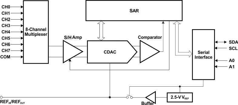
The ADS7828 is a classic Successive Approximation Register (SAR) ADC. The architecture is based on capacitive redistribution which inherently includes a sample-and-hold function. The converter is fabricated on a 0.6μ CMOS process.
The ADS7828 core is controlled by an internally generated free-running clock. When the ADS7828 is not performing conversions or being addressed, it keeps the ADC core powered off, and the internal clock does not operate.
7.2 Functional Block Diagram
7.3 Feature Description
7.3.1 Analog Input
When the converter enters the hold mode, the voltage on the selected CHx pin is captured on the internal capacitor array. The input current on the analog inputs depends on the conversion rate of the device. During the sample period, the source must charge the internal sampling capacitor (typically 25 pF). After the capacitor has been fully charged, there is no further input current. The amount of charge transfer from the analog source to the converter is a function of conversion rate.
7.3.2 Reference
The ADS7828 can operate with an internal 2.5-V reference or an external reference. If a 5-V supply is used, an external 5-V reference is required in order to provide full dynamic range for a 0 V to +VDD analog input. This external reference can be as low as 50 mV. When using a 2.7-V supply, the internal 2.5-V reference will provide full dynamic range for a 0 V to +VDD analog input.
As the reference voltage is reduced, the analog voltage weight of each digital output code is reduced. This is often referred to as the LSB (least significant bit) size and is equal to the reference voltage divided by 4096. This means that any offset or gain error inherent in the ADC will appear to increase, in terms of LSB size, as the reference voltage is reduced.
The noise inherent in the converter will also appear to increase with lower LSB size. With a 2.5-V reference, the internal noise of the converter typically contributes only 0.32 LSB peak-to-peak of potential error to the output code. When the external reference is 50 mV, the potential error contribution from the internal noise is 50 times larger—16 LSBs. The errors due to the internal noise are Gaussian in nature and can be reduced by averaging consecutive conversion results.
7.3.3 Digital Interface
The ADS7828 supports the I2C serial bus and data transmission protocol, in all three defined modes: standard, fast, and high-speed. A device that sends data onto the bus is defined as a transmitter, and a device receiving data as a receiver. The device that controls the message is called a master. The devices that are controlled by the master are slaves. The bus must be controlled by a master device that generates the serial clock (SCL), controls the bus access, and generates the Start and Stop conditions. The ADS7828 operates as a slave on the I2C bus. Connections to the bus are made via the open-drain I/O lines SDA and SCL.
The following bus protocol has been defined (see Figure 14):
- Data transfer may be initiated only when the bus is not busy.
- During data transfer, the data line must remain stable whenever the clock line is high. Changes in the data line while the clock line is high will be interpreted as control signals.
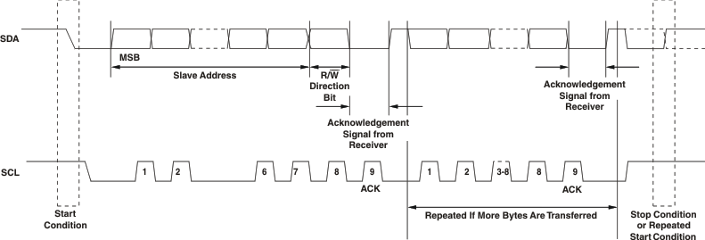 Figure 14. Basic Operation
Accordingly, the following bus conditions have been defined:
- Bus Not Busy
- Start Data Transfer
- Stop Data Transfer
- Data Valid
- Acknowledge
Both data and clock lines remain high.
A change in the state of the data line, from high to low, while the clock is high, defines a Start condition.
A change in the state of the data line, from low to high, while the clock line is high, defines the Stop condition.
The state of the data line represents valid data, when, after a Start condition, the data line is stable for the duration of the high period of the clock signal. There is one clock pulse per bit of data.
Each data transfer is initiated with a Start condition and terminated with a Stop condition. The number of data bytes transferred between Start and Stop conditions is not limited and is determined by the master device. The information is transferred byte-wise and each receiver acknowledges with a ninth-bit.
Within the I2C bus specifications a standard mode (100-kHz clock rate), a fast mode (400-kHz clock rate), and a highspeed mode (3.4-MHz clock rate) are defined. The ADS7828 works in all three modes.
Each receiving device, when addressed, is obliged to generate an acknowledge after the reception of each byte. The master device must generate an extra clock pulse that is associated with this acknowledge bit.
A device that acknowledges must pull down the SDA line during the acknowledge clock pulse in such a way that the SDA line is stable low during the high period of the acknowledge clock pulse. Of course, setup and hold times must be taken into account. A master must signal an end of data to the slave by not generating an acknowledge bit on the last byte that has been clocked out of the slave. In this case, the slave must leave the data line high to enable the master to generate the Stop condition.
Figure 14 shows how data transfer is accomplished on the I2C bus. Depending upon the state of the R/W bit, two types of data transfer are possible:
- Data transfer from a master transmitter to a slave receiver.
- Data transfer from a slave transmitter to a master receiver.
The first byte transmitted by the master is the slave address. Next follows a number of data bytes. The slave returns an acknowledge bit after the slave address and each received byte.
The first byte, the slave address, is transmitted by the master. The slave then returns an acknowledge bit. Next, a number of data bytes are transmitted by the slave to the master. The master returns an acknowledge bit after all received bytes other than the last byte. At the end of the last received byte, a not-acknowledge is returned.
The master device generates all of the serial clock pulses and the Start and Stop conditions. A transfer is ended with a Stop condition or a repeated Start condition. Since a repeated Start condition is also the beginning of the next serial transfer, the bus will not be released.
7.4 Device Functional Modes
The ADS7828 may operate in the following two modes:
- Slave Receiver Mode
- Slave Transmitter Mode
Serial data and clock are received through SDA and SCL. After each byte is received, an acknowledge bit is transmitted. Start and Stop conditions are recognized as the beginning and end of a serial transfer. Address recognition is performed by hardware after reception of the slave address and direction bit.
The first byte (the slave address) is received and handled as in the slave receiver mode. However, in this mode the direction bit will indicate that the transfer direction is reversed. Serial data is transmitted on SDA by the ADS7828 while the serial clock is input on SCL. Start and Stop conditions are recognized as the beginning and end of a serial transfer.
7.4.1 Address Byte
The address byte is the first byte received following the Start condition from the master device (see Figure 15). The first five bits (MSBs) of the slave address are factory pre-set to 10010. The next two bits of the address byte are the device select bits, A1 and A0. Input pins (A1-A0) on the ADS7828 determine these two bits of the device address for a particular ADS7828. A maximum of four devices with the same pre-set code can therefore be connected on the same bus at one time.
| MSB | 6 | 5 | 4 | 3 | 2 | 1 | LSB |
| 1 | 0 | 0 | 1 | 0 | A1 | A0 | R/W |
The A1 and A0 address inputs can be connected to VDD or digital ground. The device address is set by the state of these pins upon power-up.
The last bit of the address byte (R/W) defines the operation to be performed. When set to a 1, a read operation is selected; when set to a 0, a write operation is selected. Following the Start condition, the ADS7828 monitors the SDA bus, checking the device type identifier being transmitted. Upon receiving the 10010 code, the appropriate device select bits, and the R/W bit, the slave device outputs an acknowledge signal on the SDA line.
7.4.2 Command Byte
The operating mode is determined by a command byte (see Figure 16).
| MSB | 6 | 5 | 4 | 3 | 2 | 1 | LSB |
| SD | C2 | C1 | C0 | PD1 | PD0 | X | X |
SD: Single-ended or differential inputs
0 = Differential inputs
1 = Single-ended inputs
C2 to C0: Channel selections (see Table 1)
PD1, PD0: Power-down selection (see Table 2)
X: Unused
Table 1. Channel Selection Control Addressed by Command Byte
| COMMAND BYTE INPUTS | CHANNEL SELECTIONS | |||||||||||
|---|---|---|---|---|---|---|---|---|---|---|---|---|
| SD | C2 | C1 | C0 | CH0 | CH1 | CH2 | CH3 | CH4 | CH5 | CH6 | CH7 | COM |
| 0 | 0 | 0 | 0 | +IN | –IN | — | — | — | — | — | — | — |
| 0 | 0 | 0 | 1 | — | — | +IN | –IN | — | — | — | — | — |
| 0 | 0 | 1 | 0 | — | — | — | — | +IN | –IN | — | — | — |
| 0 | 0 | 1 | 1 | — | — | — | — | — | — | +IN | –IN | — |
| 0 | 1 | 0 | 0 | –IN | +IN | — | — | — | — | — | — | — |
| 0 | 1 | 0 | 1 | — | — | –IN | +IN | — | — | — | — | — |
| 0 | 1 | 1 | 0 | — | — | — | — | –IN | +IN | — | — | — |
| 0 | 1 | 1 | 1 | — | — | — | — | — | — | –IN | +IN | — |
| 1 | 0 | 0 | 0 | +IN | — | — | — | — | — | — | — | –IN |
| 1 | 0 | 0 | 1 | — | — | +IN | — | — | — | — | — | –IN |
| 1 | 0 | 1 | 0 | — | — | — | — | +IN | — | — | — | –IN |
| 1 | 0 | 1 | 1 | — | — | — | — | — | — | +IN | — | –IN |
| 1 | 1 | 0 | 0 | — | +IN | — | — | — | — | — | — | –IN |
| 1 | 1 | 0 | 1 | — | — | — | +IN | — | — | — | — | –IN |
| 1 | 1 | 1 | 0 | — | — | — | — | — | +IN | — | — | –IN |
| 1 | 1 | 1 | 1 | — | — | — | — | — | — | — | +IN | –IN |
Table 2. Power-Down Selection
| PD1 | PD0 | DESCRIPTION |
|---|---|---|
| 0 | 0 | Power down between ADC conversions |
| 0 | 1 | Internal reference off and ADC on |
| 1 | 0 | Internal reference on and ADC off |
| 1 | 1 | Internal reference on and ADC on |
7.4.3 Initiating Conversion
Provided the master has write-addressed it, the ADS7828 turns on the ADC section and begins conversions when it receives bit 4 of the command byte shown in Figure 16. If the command byte is correct, the ADS7828 returns an ACK condition.
7.4.4 Reading Data
Data can be read from the ADS7828 by read addressing the part (LSB of address byte set to 1) and receiving the transmitted bytes. Converted data can be read from the ADS7828 only after a conversion has been initiated as described in the preceding section.
Each 12-bit data word is returned in two bytes (see Figure 17), where D11 is the MSB of the data word, and D0 is the LSB. Byte 0 is sent first, followed by byte 1.
| MSB | 6 | 5 | 4 | 3 | 2 | 1 | LSB | |
| Byte 0 | 0 | 0 | 0 | 0 | D11 | D10 | D9 | D8 |
| Byte 1 | D7 | D6 | D5 | D4 | D3 | D2 | D1 | D0 |
7.4.5 Reading in Fast or Standard (F/S) Mode
Figure 18 shows the interaction between the master and the slave ADS7828 in fast or standard (F/S) mode. At the end of reading conversion data, the ADS7828 can be issued a repeated Start condition by the master to secure bus operation for subsequent conversions of the ADC. This would be the most efficient way to perform continuous conversions.
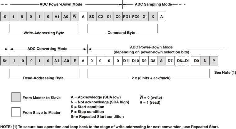 Figure 18. Typical Read Sequence in F/S Mode
7.4.6 Reading in High-Speed (HS) Mode
High Speed (HS) mode is fast enough that codes can be read out one at a time. In HS mode, there is not enough time for a single conversion to complete between the reception of a repeated Start condition and the read-addressing byte, so the ADS7828 stretches the clock after the read-addressing byte has been fully received, holding it low until the conversion is complete.
See Figure 19 for a typical read sequence for HS mode. Included in the read sequence is the shift from F/S to HS modes. It may be desirable to remain in HS mode after reading a conversion; to do this, issue a repeated Start instead of a Stop at the end of the read sequence, since a Stop causes the part to return to F/S mode.
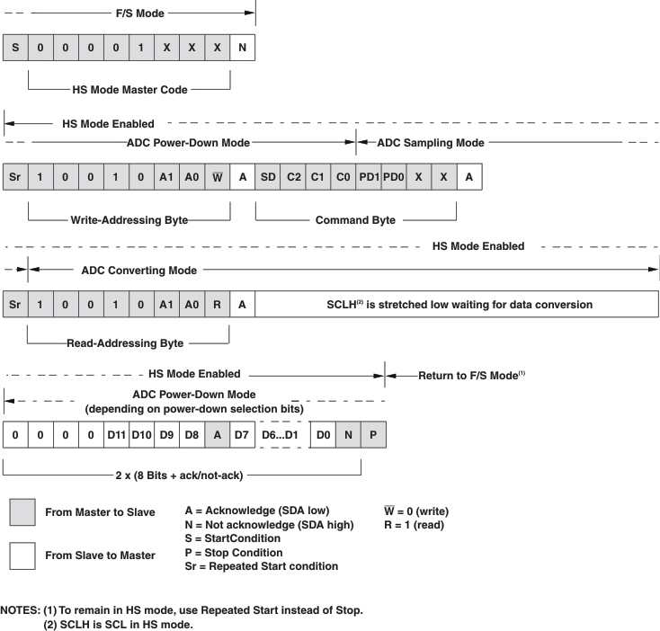 Figure 19. Typical Read Sequence in HS Mode
7.4.7 Reading With Reference On or Off
The internal reference defaults to off when the ADS7828 power is on. To turn the internal reference on or off, see Table 2. If the reference (internal or external) is constantly turned on and off, a proper amount of settling time must be added before a normal conversion cycle can be started. The exact amount of settling time needed varies depending on the configuration.
See Figure 20 for an example of the proper internal reference turn-on sequence before issuing the typical read sequences required for the F/S mode when an internal reference is used.
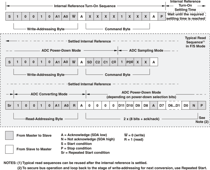 Figure 20. Internal Reference Turn-On Sequence and Typical Read Sequence (F/S Mode Shown)
When using an internal reference, there are three things that must be done:
- To use the internal reference, the PD1 bit of Command Byte must always be set to logic 1 for each sample conversion that is issued by the sequence, as shown in Figure 18.
- To achieve 12-bit accuracy conversion when using the internal reference, the internal reference settling time must be considered, as shown in the Internal VREF vs Turn-On Time Typical Characteristic plot. If the PD1 bit has been set to logic 0 while using the ADS7828, then the settling time must be reconsidered after PD1 is set to logic 1. In other words, whenever the internal reference is turned on after it has been turned off, the settling time must be long enough to get 12-bit accuracy conversion.
- When the internal reference is off, it is not turned on until both the first Command Byte with PD1 = 1 is sent and then a Stop condition or repeated Start condition is issued. (The actual turn-on time occurs once the Stop or repeated Start condition is issued.) Any Command Byte with PD1 = 1 issued after the internal reference is turned on serves only to keep the internal reference on. Otherwise, the internal reference would be turned off by any Command Byte with PD1 = 0.
The example in Figure 20 can be generalized for an HS mode conversion cycle by changing the timing of the conversion cycle. If using an external reference, PD1 must be set to 0, and the external reference must be settled. The typical sequence in Figure 18 or Figure 19 can then be used.