JAJSHX7A September 2010 – September 2019 ADS7947 , ADS7948 , ADS7949
PRODUCTION DATA.
- 1 特長
- 2 アプリケーション
- 3 概要
- 4 改訂履歴
- 5 Device Comparison Table
- 6 Pin Configuration and Functions
-
7 Specifications
- 7.1 Absolute Maximum Ratings
- 7.2 ESD Ratings
- 7.3 Recommended Operating Conditions: ADS794x (12-, 10-, 8-Bit)
- 7.4 Thermal Information
- 7.5 Electrical Characteristics: ADS7947 (12-Bit)
- 7.6 Electrical Characteristics: ADS7948 (10-Bit)
- 7.7 Electrical Characteristics: ADS7949 (8-Bit)
- 7.8 Timing Requirements
- 7.9 Switching Characteristics
- 7.10 Typical Characteristics: ADS7947, ADS7948, ADS7949
- 7.11 Typical Characteristics: ADS7947 (12-Bit)
- 8 Detailed Description
- 9 Application and Implementation
- 10Power Supply Recommendations
- 11Layout
- 12デバイスおよびドキュメントのサポート
- 13メカニカル、パッケージ、および注文情報
パッケージ・オプション
メカニカル・データ(パッケージ|ピン)
- RTE|16
サーマルパッド・メカニカル・データ
- RTE|16
発注情報
9.1.1 Driving an ADC Without a Driving Op Amp
There are some low input signal bandwidth applications, such as battery power monitoring or mains monitoring. For these applications, an ADC does not have to be operated at high sampling rates and, preferrably, avoid using a driving op amp from a cost perspective. In this case, the ADC input observes the impedance of the signal source (such as a battery or mains transformer). This section elaborates the effects of source impedance on sampling frequency.
Equation 1 can be rewritten as Equation 4:
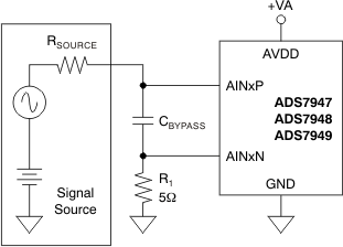
As shown in Figure 54, use a bypass capacitor across the positive and negative ADC input terminals.
 Figure 54. Driving an ADC Without a Driving Op Amp
 Source impedance (RSOURCE + R1) with (CBYPASS + CSAMPLE) acts as a low-pass filter with Equation 5:
where
Table 1 lists the recommended bypass capacitor values and the filter time constant for different source resistances. Use a 10-pF bypass capacitor, at minimum.
Table 1. Filter Time Constant versus Source Resistance
| RSOURCE (Ω) | RSOURCE + R1 | APPROXIMATE CBYPASS (pF) | CBYPASS + CSAMPLE (pF) | FILTER TIME CONSTANT (ns) |
|---|---|---|---|---|
| 15 | 20 | 370 | 400 | 8 |
| 25 | 30 | 235 | 267 | 8 |
| 50 | 55 | 115 | 145 | 8 |
| 100 | 105 | 44 | 76 | 8 |
| 180 | 185 | 10 | 43.2 | 8 |
| 250 | 255 | 10 | 42 | 10.7 |
| 1000 | 1005 | 10 | 42 | 42.2 |
| 5000 | 5005 | 10 | 42 | 210.2 |
Typically, settling resolution is selected as (ADC resolution + 2). For the ADS7947 (12-bit) the ideal settling resolution is 14. Using equations Equation 2 and Equation 3, the sampling time can be easily determined for a given source impedance. This resolution allows 80 ns of sampling time for a 12-bit ADC with 8 ns of filter time constant, which matches the ADS7947 specifications. For source impedances above 180 Ω, the filter time constant continues to increase beyond the 8 ns required for an 80-ns sampling time. This incrementation increases the minimum permissible sampling time for the 12-bit settling and the device must be operated at a lower sampling rate.
The device sampling rate can be maximized by using a 34-MHz clock even for lower throughputs. Table 2 shows typical calculations for the ADS7947(12-bit).
Table 2. Sampling Frequency versus Source Impedance for the ADS7947 (12-Bit)
| RSOURCE (Ω) | CBYPASS (pF) | SAMPLING TIME, tACQ (ns) | CONVERSION TIME, tCONV (ns) | CYCLE TIME, tACQ + tCONV (ns) | SAMPLING RATE (MSPS) |
|---|---|---|---|---|---|
| 180 | 10 | 80 | 397
(with 34MHz clock) |
477 | 2 |
| 250 | 10 | 107 | 397
(with 34MHz clock) |
504 | 1.98 |
| 1000 | 10 | 422 | 397
(with 34MHz clock) |
819 | 1.2 |
| 5000 | 10 | 2102 | 397
(with 34MHz clock) |
2499 | 0.4 |
An 1000-ns additional sampling time must be allowed over what is shown in Table 2 if PDEN (pin 12) is set high.