SBAS404D October 2006 – February 2016 ADS8556 , ADS8557 , ADS8558
PRODUCTION DATA.
- 1 Features
- 2 Applications
- 3 Description
- 4 Revision History
- 5 Pin Configuration and Functions
-
6 Specifications
- 6.1 Absolute Maximum Ratings
- 6.2 ESD Ratings
- 6.3 Recommended Operating Conditions
- 6.4 Thermal Information
- 6.5 Electrical Characteristics: General
- 6.6 Electrical Characteristics: ADS8556
- 6.7 Electrical Characteristics: ADS8557
- 6.8 Electrical Characteristics: ADS8558
- 6.9 Power Dissipation Characteristics
- 6.10 Serial Interface Timing Requirements
- 6.11 Parallel Interface Timing Requirements (Read Access)
- 6.12 Parallel Interface Timing Requirements (Write Access)
- 6.13 Typical Characteristics
- 7 Detailed Description
- 8 Application and Implementation
- 9 Power Supply Recommendations
- 10Layout
- 11Device and Documentation Support
- 12Mechanical, Packaging, and Orderable Information
10 Layout
10.1 Layout Guidelines
All GND pins must be connected to a clean ground reference. Keep this connection as short as possible to minimize the inductance of this path. Using vias connecting the pads directly to the ground plane is recommended. In designs without ground planes, keep the ground trace as wide as possible. Avoid connections that are too close to the grounding point of a microcontroller or digital signal processor.
Depending on the circuit density on the board, placement of the analog and digital components, and the related current loops, a single solid ground plane for the entire printed circuit board (PCB) or a dedicated analog ground area can be used. In case of a separated analog ground area, ensure a low-impedance connection between the analog and digital ground of the ADC by placing a bridge underneath (or next) to the ADC. Otherwise, even short undershoots on the digital interface lower than –300 mV lead to the conduction of ESD diodes causing current flow through the substrate and degrading the analog performance.
During PCB layout, care must be taken to avoid any return currents crossing sensitive analog areas or signals.
10.2 Layout Example
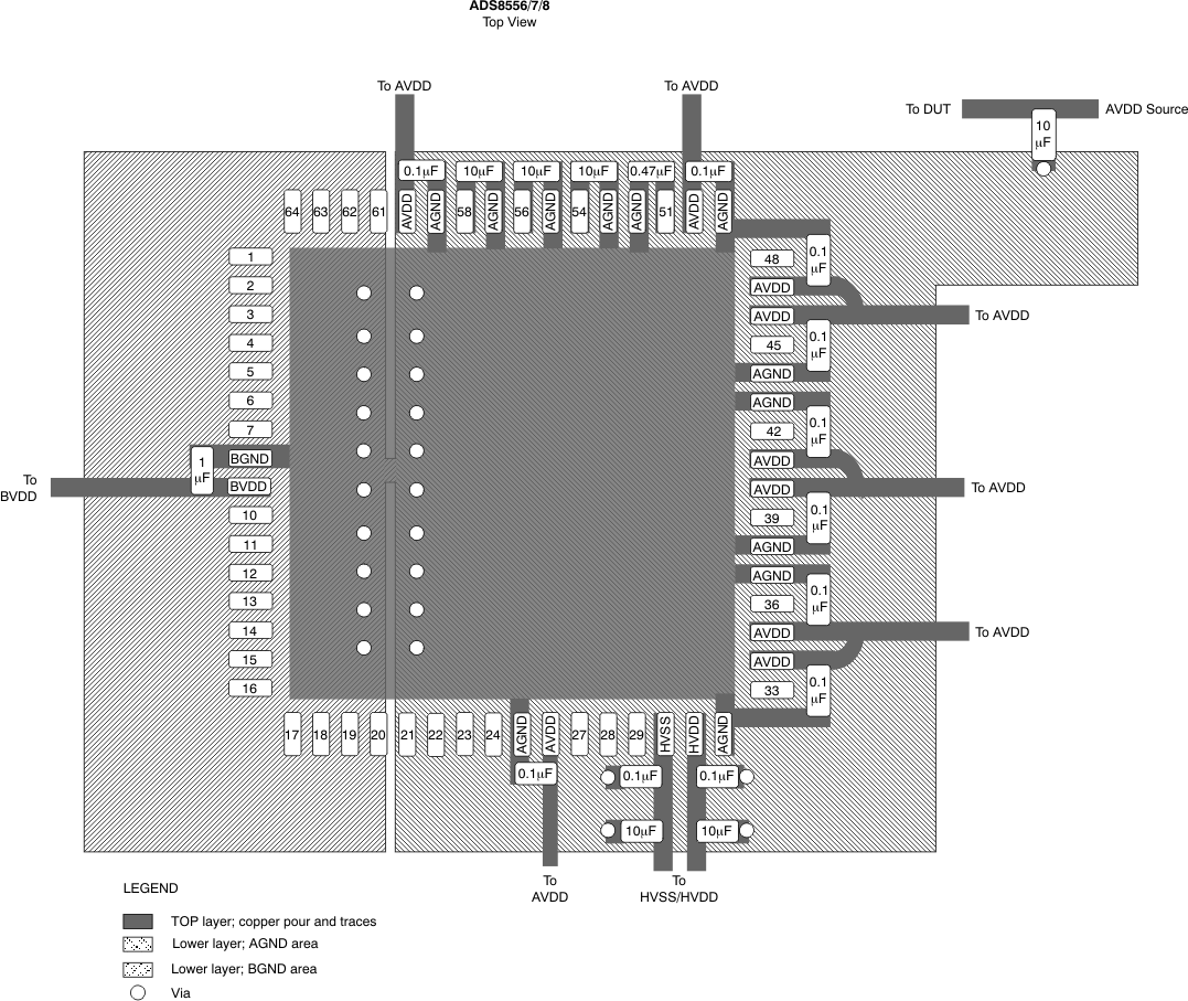
Figure 47 shows a layout recommendation for the ADS855x along with the proper decoupling and reference capacitor placement and connections.
