JAJSH04C May   2013  – March 2019 ADS8866

PRODUCTION DATA.  

  1. 特長
  2. アプリケーション
  3. 概要
    1.     Device Images
      1.      ADC 電源用に別個の LDO が不要
  4. 改訂履歴
  5. 概要(続き)
  6. Device Comparison Table
  7. Pin Configuration and Functions
    1.     Pin Functions
  8. Specifications
    1. 8.1 Absolute Maximum Ratings
    2. 8.2 ESD Ratings
    3. 8.3 Recommended Operating Conditions
    4. 8.4 Thermal Information
    5. 8.5 Electrical Characteristics
    6. 8.6 Timing Requirements: 3-Wire Operation
    7. 8.7 Timing Requirements: 4-Wire Operation
    8. 8.8 Timing Requirements: Daisy-Chain
    9. 8.9 Typical Characteristics
  9. Parameter Measurement Information
    1. 9.1 Equivalent Circuits
  10. 10Detailed Description
    1. 10.1 Overview
    2. 10.2 Functional Block Diagram
    3. 10.3 Feature Description
      1. 10.3.1 Analog Input
      2. 10.3.2 Reference
      3. 10.3.3 Clock
      4. 10.3.4 ADC Transfer Function
    4. 10.4 Device Functional Modes
      1. 10.4.1 CS Mode
        1. 10.4.1.1 3-Wire CS Mode
        2. 10.4.1.2 4-Wire CS Mode
      2. 10.4.2 Daisy-Chain Mode
        1. 10.4.2.1 Daisy-Chain Mode
  11. 11Application and Implementation
    1. 11.1 Application Information
      1. 11.1.1 ADC Reference Driver
      2. 11.1.2 ADC Input Driver
        1. 11.1.2.1 Input Amplifier Selection
        2. 11.1.2.2 Charge-Kickback Filter
    2. 11.2 Typical Applications
      1. 11.2.1 DAQ Circuit for a 10-µs, Full-Scale Step Response
        1. 11.2.1.1 Design Requirements
        2. 11.2.1.2 Detailed Design Procedure
      2. 11.2.2 DAQ Circuit for Lowest Distortion and Noise Performance at 100 kSPS
        1. 11.2.2.1 Design Requirements
        2. 11.2.2.2 Detailed Design Procedure
      3. 11.2.3 Ultralow-Power DAQ Circuit at 10 kSPS
        1. 11.2.3.1 Design Requirements
        2. 11.2.3.2 Detailed Design Procedure
  12. 12Power Supply Recommendations
    1. 12.1 Power-Supply Decoupling
    2. 12.2 Power Saving
  13. 13Layout
    1. 13.1 Layout Guidelines
    2. 13.2 Layout Example
  14. 14デバイスおよびドキュメントのサポート
    1. 14.1 ドキュメントのサポート
      1. 14.1.1 関連資料
    2. 14.2 ドキュメントの更新通知を受け取る方法
    3. 14.3 コミュニティ・リソース
    4. 14.4 商標
    5. 14.5 静電気放電に関する注意事項
    6. 14.6 Glossary
  15. 15メカニカル、パッケージ、および注文情報

パッケージ・オプション

メカニカル・データ(パッケージ|ピン)
サーマルパッド・メカニカル・データ
発注情報

Timing Requirements: Daisy-Chain

all specifications are at AVDD = 3 V, DVDD = 3 V, and over the operating free-air temperature range (unless otherwise noted)
MIN TYP MAX UNIT
tACQ Acquisition time 1200 ns
tconv Conversion time 500 8800 ns
1/fsample Time between conversions 10000 ns
tsu-CK-CNV Setup time: SCLK valid to CONVST rising edge 5 ns
th-CK-CNV Hold time: SCLK valid from CONVST rising edge 5 ns
tsu-DI-CNV Setup time: DIN low to CONVST rising edge (see Figure 2) 7.5 ns
th-DI-CNV Hold time: DIN low from CONVST rising edge 0 ns
tsu-DI-CK Setup time: DIN valid to SCLK falling edge 1.5 ns
ADS8866 tim_3wire_op_bas557.gifFigure 1. 3-Wire Operation: CONVST Functions as Chip Select
ADS8866 tim_4wire_op_bas557.gifFigure 2. 4-Wire Operation: DIN Functions as Chip Select
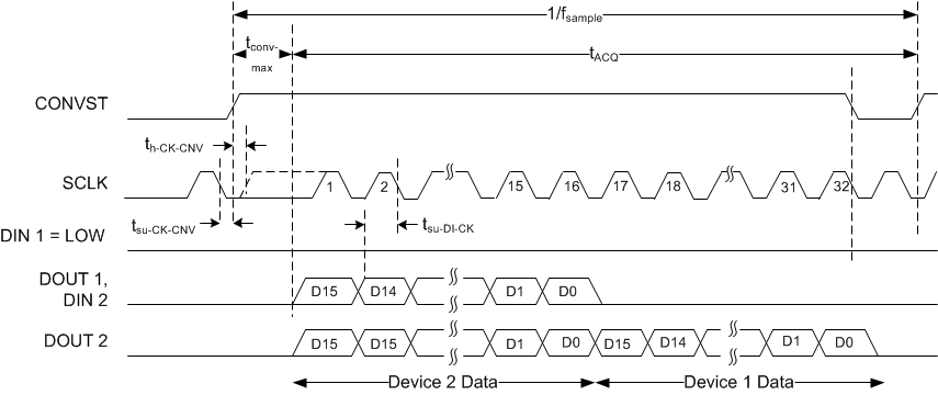
ADS8866 tim_daisy_op_bas557.gifFigure 3. Daisy-Chain Operation: Two Devices