JAJSH04C May   2013  – March 2019 ADS8866

PRODUCTION DATA.  

  1. 特長
  2. アプリケーション
  3. 概要
    1.     Device Images
      1.      ADC 電源用に別個の LDO が不要
  4. 改訂履歴
  5. 概要(続き)
  6. Device Comparison Table
  7. Pin Configuration and Functions
    1.     Pin Functions
  8. Specifications
    1. 8.1 Absolute Maximum Ratings
    2. 8.2 ESD Ratings
    3. 8.3 Recommended Operating Conditions
    4. 8.4 Thermal Information
    5. 8.5 Electrical Characteristics
    6. 8.6 Timing Requirements: 3-Wire Operation
    7. 8.7 Timing Requirements: 4-Wire Operation
    8. 8.8 Timing Requirements: Daisy-Chain
    9. 8.9 Typical Characteristics
  9. Parameter Measurement Information
    1. 9.1 Equivalent Circuits
  10. 10Detailed Description
    1. 10.1 Overview
    2. 10.2 Functional Block Diagram
    3. 10.3 Feature Description
      1. 10.3.1 Analog Input
      2. 10.3.2 Reference
      3. 10.3.3 Clock
      4. 10.3.4 ADC Transfer Function
    4. 10.4 Device Functional Modes
      1. 10.4.1 CS Mode
        1. 10.4.1.1 3-Wire CS Mode
        2. 10.4.1.2 4-Wire CS Mode
      2. 10.4.2 Daisy-Chain Mode
        1. 10.4.2.1 Daisy-Chain Mode
  11. 11Application and Implementation
    1. 11.1 Application Information
      1. 11.1.1 ADC Reference Driver
      2. 11.1.2 ADC Input Driver
        1. 11.1.2.1 Input Amplifier Selection
        2. 11.1.2.2 Charge-Kickback Filter
    2. 11.2 Typical Applications
      1. 11.2.1 DAQ Circuit for a 10-µs, Full-Scale Step Response
        1. 11.2.1.1 Design Requirements
        2. 11.2.1.2 Detailed Design Procedure
      2. 11.2.2 DAQ Circuit for Lowest Distortion and Noise Performance at 100 kSPS
        1. 11.2.2.1 Design Requirements
        2. 11.2.2.2 Detailed Design Procedure
      3. 11.2.3 Ultralow-Power DAQ Circuit at 10 kSPS
        1. 11.2.3.1 Design Requirements
        2. 11.2.3.2 Detailed Design Procedure
  12. 12Power Supply Recommendations
    1. 12.1 Power-Supply Decoupling
    2. 12.2 Power Saving
  13. 13Layout
    1. 13.1 Layout Guidelines
    2. 13.2 Layout Example
  14. 14デバイスおよびドキュメントのサポート
    1. 14.1 ドキュメントのサポート
      1. 14.1.1 関連資料
    2. 14.2 ドキュメントの更新通知を受け取る方法
    3. 14.3 コミュニティ・リソース
    4. 14.4 商標
    5. 14.5 静電気放電に関する注意事項
    6. 14.6 Glossary
  15. 15メカニカル、パッケージ、および注文情報

パッケージ・オプション

メカニカル・データ(パッケージ|ピン)
サーマルパッド・メカニカル・データ
発注情報

Reference

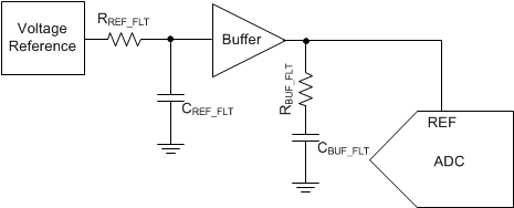
The device operates with an external reference voltage and switches binary-weighted capacitors onto the reference terminal (REF pin) during the conversion process. The switching frequency is proportional to the internal conversion clock frequency but the dynamic charge requirements are a function of the absolute value of the input voltage and reference voltage. This dynamic load must be supported by a reference driver circuit without degrading the noise and linearity performance of the device. During the acquisition process, the device automatically powers down and does not take any dynamic current from the external reference source. The basic circuit diagram for such a reference driver circuit for precision ADCs is shown in Figure 41; see the ADC Reference Driver section for more details on the application circuits.
ADS8866 ai_ref_driver_sch_bas557.gifFigure 41. Reference Driver Schematic