SBAS547D May 2013 – August 2015 ADS8881
PRODUCTION DATA.
- 1 Features
- 2 Applications
- 3 Description
- 4 Revision History
- 5 Companion Products
- 6 Device Comparison
- 7 Pin Configurations and Functions
- 8 Specifications
- 9 Parametric Measurement Information
- 10Detailed Description
-
11Application and Implementation
- 11.1 Application Information
- 11.2 Typical Applications
- 12Power-Supply Recommendations
- 13Layout
- 14Device and Documentation Support
- 15Mechanical, Packaging, and Orderable Information
パッケージ・オプション
メカニカル・データ(パッケージ|ピン)
サーマルパッド・メカニカル・データ
- DRC|10
発注情報
10 Detailed Description
10.1 Overview
The ADS8881 is a high-speed, successive approximation register (SAR), analog-to-digital converter (ADC) from a 16- and 18-bit device family. This compact device features high performance. Power consumption is inherently low and scales linearly with sampling speed. The architecture is based on charge redistribution that inherently includes a sample-and-hold (S/H) function.
The ADS8881 supports a true-differential analog input across two pins (INP and INN). When a conversion is initiated, the differential input on these pins is sampled on the internal capacitor array. While a conversion is in progress, both the INP and INN inputs are disconnected from the internal circuit.
The ADS8881 uses an internal clock to perform conversions. The device reconnects the sampling capacitors to the INP and INN pins after conversion and then enters an acquisition phase. During the acquisition phase, the device is powered down and the conversion result can be read.
The device digital output is available in SPI-compatible format, thus making interfacing with microprocessors, digital signal processors (DSPs), or field-programmable gate arrays (FPGAs) easy.
10.2 Functional Block Diagram
Figure 45 shows the detailed functional block diagram for the device.
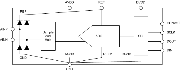 Figure 45. Detailed Block Diagram
10.3 Feature Description
10.3.1 Analog Input
As shown in Figure 45, the device features a differential analog input. Both positive and negative inputs are individually sampled on 55-pF sampling capacitors and the device converts for the voltage difference between the two sampled values: VINP – VINN.
Most differential input SAR ADCs prohibit the input common-mode voltage, VCM (that is, the average voltage between the inputs), at AINP or AINM from varying more than approximately 10% beyond the mid-scale input value. As shown in Figure 46, the device has a unique common-mode voltage detection and rejection block that does not have this restriction and thus allows VCM to be set to any value between 0 V and VREF without degrading device performance.
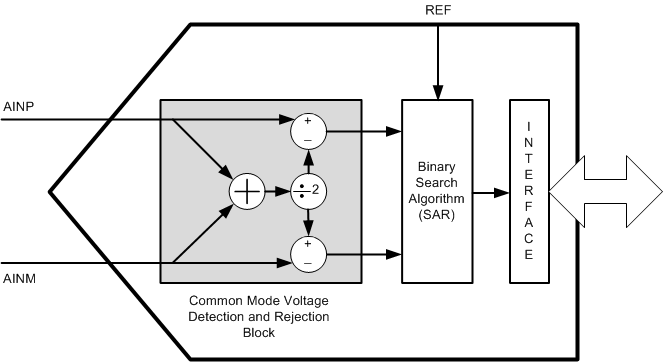 Figure 46. Conceptual Diagram: True Differential Input Structure
Table 1 shows the full-scale input range of the device as a function of input common-mode voltage. The device offers a maximum dynamic range for VCM = VREF / 2. The differential input with wide common-mode range allows connecting differential signals from sensors without any signal conditioning.
Table 1. Full-Scale Input Range
| VCM | ABSOLUTE INPUT RANGE | FULL SCALE INPUT RANGE (VFS) | |
|---|---|---|---|
| VAINP | VAINN | ||
| VCM < VREF / 2 | 0 to 2 × VCM | 0 to 2 × VCM | (–2 × VCM) to (2 × VCM) |
| VCM = VREF / 2 | 0 to VREF | 0 to VREF | (–VREF) to (VREF) |
| VCM > VREF / 2 | (2 × VCM – VREF) to VREF | (2 × VCM – VREF) to VREF | [–2 × (VCM – VREF)] to [2 × (VCM – VREF)] |
Figure 47 shows an equivalent circuit of the input sampling stage. The sampling switch is represented by a 96-Ω resistance in series with the ideal switch; see the ADC Input Driver section for more details on the recommended driving circuits.
 Figure 47. Input Sampling Stage Equivalent Circuit
Figure 45 and Figure 47 illustrate electrostatic discharge (ESD) protection diodes to REF and GND from both analog inputs. Make sure that these diodes do not turn on by keeping the analog inputs within the specified range.
10.3.2 Reference
The device operates with an external reference voltage and switches binary-weighted capacitors onto the reference terminal (REF pin) during the conversion process. The switching frequency is proportional to the internal conversion clock frequency but the dynamic charge requirements are a function of the absolute value of the input voltage and reference voltage. This dynamic load must be supported by a reference driver circuit without degrading the noise and linearity performance of the device. During the acquisition process, the device automatically powers down and does not take any dynamic current from the external reference source. The basic circuit diagram for such a reference driver circuit for precision ADCs is shown in Figure 48; see the ADC Reference Driver section for more details on the application circuits.
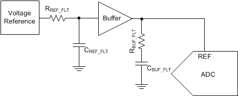 Figure 48. Reference Driver Schematic
10.3.3 Clock
The device uses an internal clock for conversion. Conversion duration may vary but is bounded by the minimum and maximum value of tconv, as specified in the Timing Requirements section. An external SCLK is only used for a serial data read operation. Data are read after a conversion completes and when the device is in acquisition phase for the next sample.
10.3.4 ADC Transfer Function
The ADS8881 is a unipolar, differential input device. The device output is in twos compliment format.
Figure 49 shows ideal characteristics for the device. The full-scale range for the ADC input (AINP – AINN) is equal to twice the reference input voltage to the ADC (2 × VREF). The LSB for the ADC is given by Equation 1.
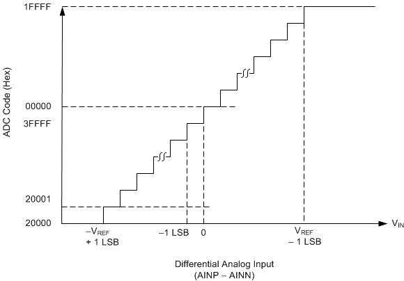 Figure 49. Differential Transfer Characteristics
10.4 Device Functional Modes
The ADS8881 is a low pin-count device. However, the device offers six different options for interfacing with the digital host.
These options can be broadly classified as being either CS mode (in either a 3- or 4-wire interface) or daisy-chain mode. The device operates in CS mode if DIN is high at the CONVST rising edge. If DIN is low at the CONVST rising edge, or if DIN and CONVST are connected together, the device operates in daisy-chain mode. In both modes, the device can either operate with or without a busy indicator, where the busy indicator is a bit preceding the output data bits that can be used to interrupt the digital host and trigger the data transfer.
The 3-wire interface in CS mode is useful for applications that need galvanic isolation on-board. The 4-wire interface in CS mode allows the user to sample the analog input independent of the serial interface timing and, therefore, allows easier control of an individual device while having multiple, similar devices on-board. The daisy-chain mode is provided to hook multiple devices in a chain similar to a shift register and is useful in reducing component count and the number of signal traces on the board.
10.4.1 CS Mode
CS mode is selected if DIN is high at the CONVST rising edge. There are four different interface options available in this mode: 3-wire CS mode without a busy indicator, 3-wire CS mode with a busy indicator, 4-wire CS mode without a busy indicator, and 4-wire CS mode with a busy indicator. The following sections discuss these interface options in detail.
10.4.1.1 3-Wire CS Mode Without a Busy Indicator
This interface option is most useful when a single ADC is connected to an SPI-compatible digital host. In this interface option, DIN can be connected to DVDD and CONVST functions as CS (as shown in Figure 50). As shown in Figure 51, a CONVST rising edge forces DOUT to 3-state, samples the input signal, and causes the device to enter a conversion phase. Conversion is done with the internal clock and continues regardless of the state of CONVST. As a result, CONVST (functioning as CS) can be pulled low after the start of the conversion to select other devices on the board. However, CONVST must return high before the minimum conversion time (tconv-min) elapses and is held high until the maximum possible conversion time (tconv-max) elapses. A high level on CONVST at the end of the conversion ensures the device does not generate a busy indicator.
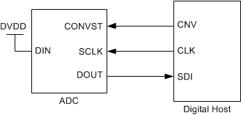 Figure 50. Connection Diagram: 3-Wire CS Mode Without a Busy Indicator (DIN = 1)
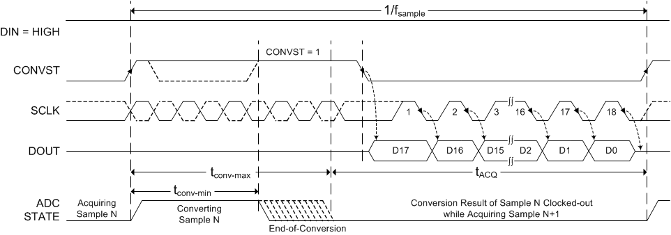 Figure 51. Interface Timing Diagram: 3-Wire CS Mode (DIN = 1)
When conversion is complete, the device enters an acquisition phase and powers down. CONVST (functioning as CS) can be brought low after the maximum conversion time (tconv-max) elapses. On the CONVST falling edge, DOUT comes out of 3-state and the device outputs the MSB of the data. The lower data bits are output on subsequent SCLK falling edges. Fast sampling rates require high frequency SCLK and data must be read at SCLK falling edges. For slow sampling rates and SCLK frequency ≤ 36 MHz, data can be read at either SCLK falling or rising edges. Note that with any SCLK frequency, reading data at SCLK falling edge requires the digital host to clock in the data during the th_CK_DO-min time frame. DOUT goes to 3-state after the 18th SCLK falling edge or when CONVST goes high, whichever occurs first.
10.4.1.2 3-Wire CS Mode With a Busy Indicator
This interface option is most useful when a single ADC is connected to an SPI-compatible digital host and an interrupt-driven data transfer is desired. In this interface option, DIN can be connected to DVDD and CONVST functions as CS (as shown in Figure 52). The pull-up resistor on the DOUT pin ensures that the IRQ pin of the digital host is held high when DOUT goes to 3-state. As shown in Figure 53, a CONVST rising edge forces DOUT to 3-state, samples the input signal, and causes the device to enter a conversion phase. Conversion is done with the internal clock and continues regardless of the state of CONVST. As a result, CONVST (functioning as CS) can be pulled low after the start of the conversion to select other devices on the board. However, CONVST must be pulled low before the minimum conversion time (tconv-min) elapses and must remain low until the maximum possible conversion time (tconv-max) elapses. A low level on the CONVST input at the end of a conversion ensures the device generates a busy indicator.
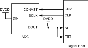 Figure 52. Connection Diagram: 3-Wire CS Mode With a Busy Indicator
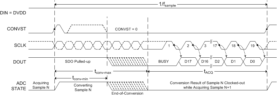 Figure 53. Interface Timing Diagram: 3-Wire CS Mode With a Busy Indicator (DIN = 1)
When conversion is complete, the device enters an acquisition phase and powers down, DOUT comes out of 3-state, and the device outputs a busy indicator bit (low level) on the DOUT pin. This configuration provides a high-to-low transition on the IRQ pin of the digital host. The data bits are clocked out, MSB first, on the subsequent SCLK falling edges. Fast sampling rates require high frequency SCLK and data must be read at SCLK falling edges. For slow sampling rates and SCLK frequency ≤ 36 MHz, data can be read at either SCLK falling or rising edges. Note that with any SCLK frequency, reading data at SCLK falling edge requires the digital host to clock in the data during the th_CK_DO-min time frame. DOUT goes to 3-state after the 19th SCLK falling edge or when CONVST goes high, whichever occurs first.
10.4.1.3 4-Wire CS Mode Without a Busy Indicator
This interface option is useful when one or more ADCs are connected to an SPI-compatible digital host. Figure 54 shows the connection diagram for single ADC; see Figure 56 for the connection diagram for two ADCs.
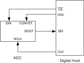 Figure 54. Connection Diagram: Single ADC With 4-Wire CS Mode Without a Busy Indicator
In this interface option, DIN is controlled by the digital host and functions as CS. As shown in Figure 55, with DIN high, a CONVST rising edge selects CS mode, forces DOUT to 3-state, samples the input signal, and causes the device to enter a conversion phase. In this interface option, CONVST must be held at a high level from the start of the conversion until all data bits are read. Conversion is done with the internal clock and continues regardless of the state of DIN. As a result, DIN (functioning as CS) can be pulled low to select other devices on the board. However, DIN must be pulled high before the minimum conversion time (tconv-min) elapses and remains high until the maximum possible conversion time (tconv-max) elapses. A high level on DIN at the end of the conversion ensures the device does not generate a busy indicator.
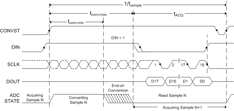 Figure 55. Interface Timing Diagram: Single ADC With 4-Wire CS Mode
When conversion is complete, the device enters acquisition phase and powers down. DIN (functioning as CS) can be brought low after the maximum conversion time (tconv-max) elapses. On the DIN falling edge, DOUT comes out of 3-state and the device outputs the MSB of the data. The lower data bits are output on subsequent SCLK falling edges. Fast sampling rates require high frequency SCLK and data must be read at SCLK falling edges. For slow sampling rates and SCLK frequency ≤ 36 MHz, data can be read at either SCLK falling or rising edges. Note that with any SCLK frequency, reading data at SCLK falling edge requires the digital host to clock in the data during the th_CK_DO-min time frame. DOUT goes to 3-state after the 18th SCLK falling edge or when DIN goes high, whichever occurs first.
As shown in Figure 56, multiple devices can be hooked together on the same data bus. In this case, as shown in Figure 57, the DIN of the second device (functioning as CS for the second device) can go low after the first device data are read and the DOUT of the first device is in 3-state.
Care must be taken so that CONVST and DIN are not both low together at any time during the cycle.
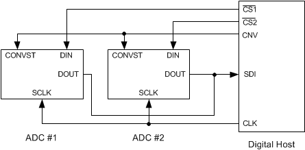 Figure 56. Connection Diagram: Two ADCs With 4-Wire CS Mode Without a Busy Indicator
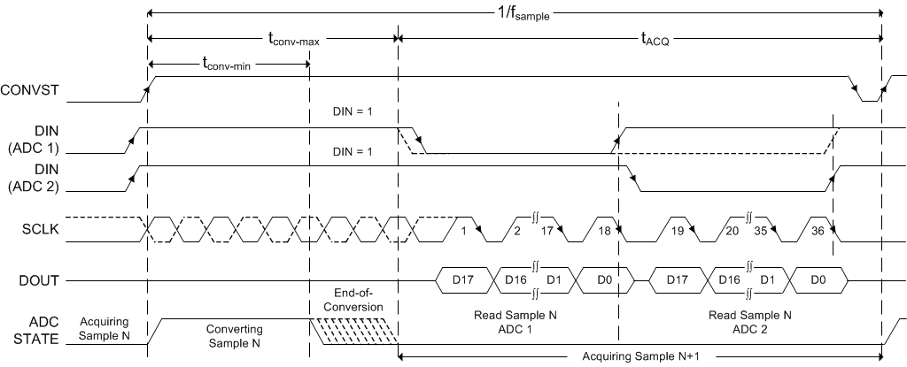 Figure 57. Interface Timing Diagram: Two ADCs With 4-Wire CS Mode
10.4.1.4 4-Wire CS Mode With a Busy Indicator
This interface option is most useful when a single ADC is connected to an SPI-compatible digital host and an interrupt-driven data transfer is desired. In this interface option, the analog sample is least affected by clock jitter because the CONVST signal (used to sample the input) is independent of the data read operation. In this interface option, DIN is controlled by the digital host and functions as CS (as shown in Figure 58). The pull-up resistor on the DOUT pin ensures that the IRQ pin of the digital host is held high when DOUT goes to 3-state. As shown in Figure 59, when DIN is high, a CONVST rising edge selects CS mode, forces DOUT to 3-state, samples the input signal, and causes the device to enter a conversion phase. In this interface option, CONVST must be held high from the start of the conversion until all data bits are read. Conversion is done with the internal clock and continues regardless of the state of DIN. As a result, DIN (acting as CS) can be pulled low to select other devices on the board. However, DIN must be pulled low before the minimum conversion time (tconv-min) elapses and remains low until the maximum possible conversion time (tconv-max) elapses. A low level on the DIN input at the end of a conversion ensures the device generates a busy indicator.
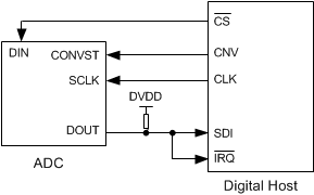 Figure 58. Connection Diagram: 4-Wire CS Mode With a Busy Indicator
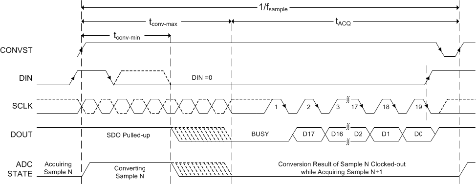 Figure 59. Interface Timing Diagram: 4-Wire CS Mode With a Busy Indicator
When conversion is complete, the device enters an acquisition phase and powers down, DOUT comes out of 3-state, and the device outputs a busy indicator bit (low level) on the DOUT pin. This configuration provides a high-to-low transition on the IRQ pin of the digital host. The data bits are clocked out, MSB first, on the subsequent SCLK falling edges. Fast sampling rates require high frequency SCLK and data must be read at SCLK falling edges. For slow sampling rates and SCLK frequency ≤ 36 MHz, data can be read at either SCLK falling or rising edges. Note that with any SCLK frequency, reading data at SCLK falling edge requires the digital host to clock in the data during the th_CK_DO-min time frame. DOUT goes to 3-state after the 19th SCLK falling edge or when DIN goes high, whichever occurs first. Care must be taken so that CONVST and DIN are not both low together at any time during the cycle.
10.4.2 Daisy-Chain Mode
Daisy-chain mode is selected if DIN is low at the time of a CONVST rising edge or if DIN and CONVST are connected together. Similar to CS mode, this mode features operation with or without a busy indicator. The following sections discuss these interface modes in detail.
10.4.2.1 Daisy-Chain Mode Without a Busy Indicator
This interface option is most useful in applications where multiple ADC devices are used but the digital host has limited interfacing capability. Figure 60 shows a connection diagram with N ADCs connected in the daisy-chain. The CONVST pins of all ADCs in the chain are connected together and are controlled by a single pin of the digital host. Similarly, the SCLK pins of all ADCs in the chain are connected together and are controlled by a single pin of the digital host. The DIN pin for ADC 1 (DIN-1) is connected to GND. The DOUT pin of ADC 1 (DOUT-1) is connected to the DIN pin of ADC 2 (DIN-2), and so on. The DOUT pin of the last ADC in the chain (DOUT-N) is connected to the SDI pin of the digital host.
 Figure 60. Connection Diagram: Daisy-Chain Mode Without a Busy Indicator (DIN = 0)
As shown in Figure 61, the device DOUT pin is driven low when DIN and CONVST are low together. With DIN low, a CONVST rising edge selects daisy-chain mode, samples the analog input, and causes the device to enter a conversion phase. In this interface option, CONVST must remain high from the start of the conversion until all data bits are read. When started, the conversion continues regardless of the state of SCLK, however SCLK must be low at the CONVST rising edge so that the device does not generate a busy indicator at the end of the conversion.
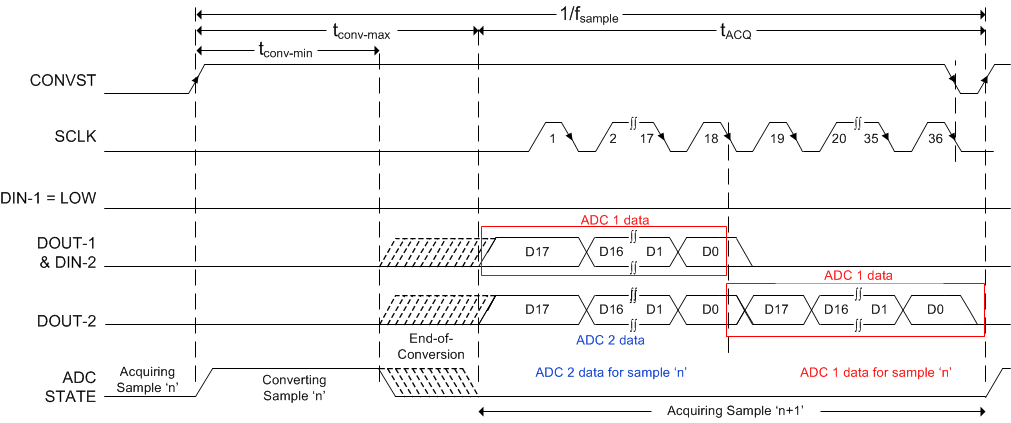 Figure 61. Interface Timing Diagram: For Two Devices in Daisy-Chain Mode
At the end of conversion, every ADC in the chain loads its own conversion result into the internal, 18-bit, shift register and also outputs the MSB bit of this conversion result on its own DOUT pin. All ADCs enter an acquisition phase and power-down. On every subsequent SCLK falling edge, the internal shift register of each ADC latches the data available on its DIN pin and shifts out the next bit of data on its DOUT pin. Therefore, the digital host receives the data of ADC N, followed by the data of ADC N–1, and so on (in MSB-first fashion). A total of 18 x N SCLK falling edges are required to capture the outputs of all N devices in the chain. Fast sampling rates require high frequency SCLK and data must be read at SCLK falling edges. For slow sampling rates and SCLK frequency ≤ 36 MHz, data can be read at either SCLK falling or rising edges. Note that with any SCLK frequency, reading data at SCLK falling edge requires the digital host to clock in the data during the th_CK_DO-min time frame.
10.4.2.2 Daisy-Chain Mode With a Busy Indicator
This interface option is most useful in applications where multiple ADC devices are used but the digital host has limited interfacing capability and an interrupt-driven data transfer is desired. Figure 62 shows a connection diagram with N ADCs connected in the daisy-chain. The CONVST pins of all ADCs in the chain are connected together and are controlled by a single pin of the digital host. Similarly, the SCLK pins of all ADCs in the chain are connected together and are controlled by a single pin of the digital host. The DIN pin for ADC 1 (DIN-1) is connected to its CONVST. The DOUT pin of ADC 1 (DOUT-1) is connected to the DIN pin of ADC 2 (DIN-2), and so on. The DOUT pin of the last ADC in the chain (DOUT-N) is connected to the SDI and IRQ pins of the digital host.
 Figure 62. Connection Diagram: Daisy-Chain Mode With a Busy Indicator (DIN = 0)
As shown in Figure 63, the device DOUT pin is driven low when DIN and CONVST are low together. A CONVST rising edge selects daisy-chain mode, samples the analog input, and causes the device to enter a conversion phase. In this interface option, CONVST must remain high from the start of the conversion until all data bits are read. When started, the conversion continues regardless of the state of SCLK, however SCLK must be high at the CONVST rising edge so that the device generates a busy indicator at the end of the conversion.
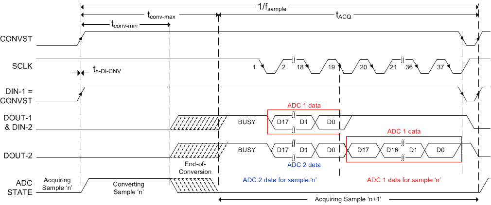 Figure 63. Interface Timing Diagram: For Two Devices in Daisy-Chain Mode With a Busy Indicator
At the end of conversion, every ADC in the chain loads its own conversion result into the internal, 18-bit, shift register and also forces its DOUT pin high, thereby providing a low-to-high transition on the IRQ pin of the digital host. All ADCs enter an acquisition phase and power-down. On every subsequent SCLK falling edge, the internal shift register of each ADC latches the data available on its DIN pin and shifts out the next bit of data on its DOUT pin. Therefore, the digital host receives the interrupt signal followed by the data of ADC N followed by the data of ADC N–1, and so on (in MSB-first fashion). A total of (18 × N) + 1 SCLK falling edges are required to capture the outputs of all N devices in the chain. Fast sampling rates require a high-frequency SCLK and data must be read at the SCLK falling edges. For slow sampling rates and SCLK frequency ≤ 36 MHz, data can be read at either SCLK falling or rising edges. Note that with any SCLK frequency, reading data at the SCLK falling edge requires the digital host to clock in the data during the th_CK_DO-min time frame. Note that the busy indicator bits of ADC 1 to ADC N–1 do not propagate to the next device in the chain.
NOTE: For SCLK ≤ 36 MHz, SPI mode-3 (CPOL = 1, CPHA = 1) allows reading the conversion results of N ADCs in 18 × N SCLK cycles because the busy indicator bit is not clocked in by the host.