SBAS547D May   2013  – August 2015 ADS8881

PRODUCTION DATA.  

  1. Features
  2. Applications
  3. Description
  4. Revision History
  5. Companion Products
  6. Device Comparison
  7. Pin Configurations and Functions
  8. Specifications
    1. 8.1 Absolute Maximum Ratings
    2. 8.2 ESD Ratings
    3. 8.3 Recommended Operating Conditions
    4. 8.4 Thermal Information
    5. 8.5 Electrical Characteristics
    6. 8.6 Timing Requirements: 3-Wire Operation
    7. 8.7 Timing Requirements: 4-Wire Operation
    8. 8.8 Timing Requirements: Daisy-Chain
    9. 8.9 Typical Characteristics
  9. Parametric Measurement Information
    1. 9.1 Equivalent Circuits
  10. 10Detailed Description
    1. 10.1 Overview
    2. 10.2 Functional Block Diagram
    3. 10.3 Feature Description
      1. 10.3.1 Analog Input
      2. 10.3.2 Reference
      3. 10.3.3 Clock
      4. 10.3.4 ADC Transfer Function
    4. 10.4 Device Functional Modes
      1. 10.4.1 CS Mode
        1. 10.4.1.1 3-Wire CS Mode Without a Busy Indicator
        2. 10.4.1.2 3-Wire CS Mode With a Busy Indicator
        3. 10.4.1.3 4-Wire CS Mode Without a Busy Indicator
        4. 10.4.1.4 4-Wire CS Mode With a Busy Indicator
      2. 10.4.2 Daisy-Chain Mode
        1. 10.4.2.1 Daisy-Chain Mode Without a Busy Indicator
        2. 10.4.2.2 Daisy-Chain Mode With a Busy Indicator
  11. 11Application and Implementation
    1. 11.1 Application Information
      1. 11.1.1 ADC Reference Driver
      2. 11.1.2 ADC Input Driver
        1. 11.1.2.1 Input Amplifier Selection
        2. 11.1.2.2 Antialiasing Filter
    2. 11.2 Typical Applications
      1. 11.2.1 DAQ Circuit for a 1-µs, Full-Scale Step Response
        1. 11.2.1.1 Design Requirements
        2. 11.2.1.2 Detailed Design Procedure
        3. 11.2.1.3 Application Curve
      2. 11.2.2 Low-Power DAQ Circuit for Excellent Dynamic Performance at 1 MSPS
        1. 11.2.2.1 Design Requirements
        2. 11.2.2.2 Detailed Design Procedure
        3. 11.2.2.3 Application Curve
      3. 11.2.3 DAQ Circuit for Lowest Distortion and Noise Performance at 1 MSPS
        1. 11.2.3.1 Design Requirements
        2. 11.2.3.2 Detailed Design Procedure
        3. 11.2.3.3 Application Curve
      4. 11.2.4 Ultralow-Power DAQ Circuit at 10 kSPS
        1. 11.2.4.1 Design Requirements
        2. 11.2.4.2 Detailed Design Procedure
        3. 11.2.4.3 Application Curve
  12. 12Power-Supply Recommendations
    1. 12.1 Power-Supply Decoupling
    2. 12.2 Power Saving
  13. 13Layout
    1. 13.1 Layout Guidelines
    2. 13.2 Layout Example
  14. 14Device and Documentation Support
    1. 14.1 Device Support
      1. 14.1.1 Development Support
    2. 14.2 Documentation Support
      1. 14.2.1 Related Documentation
    3. 14.3 Receiving Notification of Documentation Updates
    4. 14.4 Community Resources
    5. 14.5 Trademarks
    6. 14.6 Electrostatic Discharge Caution
    7. 14.7 Glossary
  15. 15Mechanical, Packaging, and Orderable Information

パッケージ・オプション

メカニカル・データ(パッケージ|ピン)
サーマルパッド・メカニカル・データ
発注情報

7 Pin Configurations and Functions

DGS Package
VSSOP-10
Top View, Not to Scale
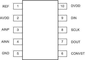
ADS8881 po_msop_bas557.gif
DRC Package
VSON-10
Top View, Not to Scale
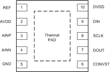
ADS8881 po_son_bas557.gif

Pin Functions

PIN I/O DESCRIPTION
NAME NO.
AINN 4 Analog input Inverting analog signal input
AINP 3 Analog input Noninverting analog signal input
AVDD 2 Analog Analog power supply. This pin must be decoupled to GND with a 1-μF capacitor.
CONVST 6 Digital input Convert input. This pin also functions as the CS input in 3-wire interface mode; see the Description and Timing Requirements sections for more details.
DIN 9 Digital input Serial data input. The DIN level at the start of a conversion selects the mode of operation (such as CS or daisy-chain mode). This pin also serves as the CS input in 4-wire interface mode; see the Description and Timing Requirements sections for more details.
DOUT 7 Digital output Serial data output
DVDD 10 Power supply Digital interface power supply. This pin must be decoupled to GND with a 1-μF capacitor.
GND 5 Analog, digital Device ground. Note that this pin is a common ground pin for both the analog power supply (AVDD) and digital I/O supply (DVDD). The reference return line is also internally connected to this pin.
REF 1 Analog Positive reference input. This pin must be decoupled with a 10-μF or larger capacitor.
SCLK 8 Digital input Clock input for serial interface. Data output (on DOUT) are synchronized with this clock.
Thermal pad Thermal pad Exposed thermal pad (only for the DRC package option). Texas Instruments recommends connecting the thermal pad to the printed circuit board (PCB) ground.