JAJSCN8A November 2016 – June 2017 ADS8900B , ADS8902B , ADS8904B
PRODUCTION DATA.
- 1 特長
- 2 アプリケーション
- 3 概要
- 4 改訂履歴
- 5 Pin Configuration and Functions
- 6 Specifications
-
7 Detailed Description
- 7.1 Overview
- 7.2 Functional Block Diagram
- 7.3 Feature Description
- 7.4 Device Functional Modes
- 7.5
Programming
- 7.5.1 Output Data Word
- 7.5.2 Data Transfer Frame
- 7.5.3 Interleaving Conversion Cycles and Data Transfer Frames
- 7.5.4 Data Transfer Protocols
- 7.5.5 Device Setup
- 7.6
Register Maps
- 7.6.1
Device Configuration and Register Maps
- 7.6.1.1 PD_CNTL Register (address = 04h) [reset = 00h]
- 7.6.1.2 SDI_CNTL Register (address = 008h) [reset = 00h]
- 7.6.1.3 SDO_CNTL Register (address = 0Ch) [reset = 00h]
- 7.6.1.4 DATA_CNTL Register (address = 010h) [reset = 00h]
- 7.6.1.5 PATN_LSB Register (address = 014h) [reset = 00h]
- 7.6.1.6 PATN_MID Register (address = 015h) [reset = 00h]
- 7.6.1.7 PATN_MSB Register (address = 016h) [reset = 00h]
- 7.6.1.8 OFST_CAL Register (address = 020h) [reset = 00h]
- 7.6.1.9 REF_MRG Register (address = 030h) [reset = 00h]
- 7.6.1
Device Configuration and Register Maps
-
8 Application and Implementation
- 8.1 Application Information
- 8.2 Typical Application
- 9 Power-Supply Recommendations
- 10Layout
- 11デバイスおよびドキュメントのサポート
- 12メカニカル、パッケージ、および注文情報
パッケージ・オプション
メカニカル・データ(パッケージ|ピン)
- RGE|24
サーマルパッド・メカニカル・データ
- RGE|24
発注情報
8 Application and Implementation
NOTE
Information in the following applications sections is not part of the TI component specification, and TI does not warrant its accuracy or completeness. TI’s customers are responsible for determining suitability of components for their purposes. Customers should validate and test their design implementation to confirm system functionality.
8.1 Application Information
The two primary circuits required to maximize the performance of a high-precision, successive approximation register (SAR), analog-to-digital converter (ADC) are the input driver and the reference driver circuits. This section presents general principles for designing these circuits, followed by an application circuit designed using the ADS890xB.
8.1.1 ADC Reference Driver
The external reference source must provide low-drift and very accurate voltage at the REFIN pin of the ADS890xB. The output broadband noise of most references can be in the order of a few hundred μVRMS. Therefore, to prevent any degradation in the noise performance of the ADC, appropriately filter the output of the voltage reference by using a low-pass filter with a cutoff frequency of a few hundred hertz.
The internal reference buffer of the ADS890xB provides the dynamic load posed on the REFBUFOUT pin during the conversion process. Decouple the REFBUFOUT pin with the REFM pin using the recommended CREFBUF and RESR. See the Layout section for layout recommendations.
8.1.2 ADC Input Driver
The input driver circuit for a high-precision ADC mainly consists of two parts: a driving amplifier and a charge kickback filter. The amplifier is used for signal conditioning of the input signal and the low output impedance of the amplifier provides a buffer between the signal source and the switched capacitor inputs of the ADC. The charge kickback filter helps attenuate the sampling charge injection from the switched-capacitor input stage of the ADC, and band-limits the wideband noise contributed by the front-end circuit. Careful design of the front-end circuit is critical to meet the linearity and noise performance of the ADS890xB.
8.1.2.1 Charge-Kickback Filter
The charge-kickback filter is an RC filter at the input pins of the ADC that filters the broadband noise from the front-end drive circuitry, and attenuates the sampling charge injection from the switched-capacitor input stage of the ADC. A filter capacitor, CFLT, is connected from each input pin of the ADC to the ground (as shown in Figure 104). This capacitor helps reduce the sampling charge injection and provides a charge bucket to quickly charge the internal sample-and-hold capacitors during the acquisition process. Generally, the value of this capacitor must be at least 20 times the specified value of the ADC sampling capacitance. For the ADS890xB, the input sampling capacitance is equal to 60 pF; therefore, for optimal performance, keep CFLT greater than 1.2 nF. This capacitor must be a COG- or NPO-type. The type of dielectric used in COG or NPO ceramic capacitors provides the most stable electrical properties over voltage, frequency, and temperature changes.
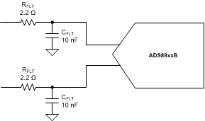 Figure 104. Charge Kickback Filter Configuration
Driving capacitive loads can degrade the phase margin of the input amplifier, thus making the amplifier marginally unstable. To avoid amplifier stability issues, series isolation resistors (RFLT) are used at the output of the amplifiers. A higher value of RFLT helps with amplifier stability, but adds distortion as a result of interactions with the nonlinear input impedance of the ADC. Distortion increases with source impedance, input signal frequency, and input signal amplitude. Therefore, the selection of RFLT requires balancing the stability of the driver amplifier and distortion performance of the design. Always verify the stability and settling behavior of the driving amplifier and charge-kickback filter by TINA-TI™ SPICE simulation. Keep the tolerance of the selected resistors less than 1% to keep the inputs balanced.
8.1.2.2 Input Amplifier Selection
Selection criteria for the input amplifiers is highly dependent on the input signal type, as well as the performance goals, of the data acquisition system. Some key amplifier specifications to consider when selecting an appropriate amplifier to drive the inputs of the ADC are:
- Small-signal bandwidth. Select the small-signal bandwidth of the input amplifiers to be as high as possible after meeting the power budget of the system. Higher bandwidth reduces the closed-loop output impedance of the amplifier, thus allowing the amplifier to more easily drive the ADC sample-and-hold capacitor and the RC filter (Charge-Kickback Filter) at the inputs of the ADC. Higher bandwidth amplifiers offer faster settling times while driving the capacitive load of the charge-kickback filter, thus reducing harmonic distortion at higher input frequencies. In order to maintain the overall stability of the input driver circuit, select the amplifier with a unity gain bandwidth (UGB) as described in Equation 16:
- Distortion. Both the ADC and the input driver introduce distortion in a data acquisition block. To make sure that the distortion performance of the data acquisition system is not limited by the front-end circuit, the distortion of the input driver must be at least 10 dB less than the distortion of the ADC, as shown in Equation 17.
- Noise. Noise contribution of the front-end amplifiers must be as low as possible to prevent any degradation in SNR performance of the system. Generally, to make sure that the noise performance of the data acquisition system is not limited by the front-end circuit, the total noise contribution from the front-end circuit must be kept below 20% of the input-referred noise of the ADC. Noise from the input driver circuit is band-limited by designing a low cutoff frequency, charge-kickback filter, as explained in Equation 18.
- V1 / f_AMP_PP is the peak-to-peak flicker noise in µV
- en_RMS is the amplifier broadband noise density in nV/√Hz
- f–3dB is the 3-dB bandwidth of the charge-kickback filter
- NG is the noise gain of the front-end circuit that is equal to 1 in a buffer configuration
- Settling Time. For dc signals with fast transients that are common in a multiplexed application, the input signal must settle within an 20-bit accuracy at the device inputs during the acquisition time window. This condition is critical to maintain the overall linearity performance of the ADC. Typically, amplifier data sheets specify the output settling performance only up to 0.1% to 0.001%, which may not be sufficient for the desired 20-bit accuracy. Therefore, always verify the settling behavior of the input driver by TINA-TI SPICE simulations before selecting the amplifier.


where
8.2 Typical Application
8.2.1 Data Acquisition (DAQ) Circuit for Lowest Distortion and Noise Performance With Differential Input
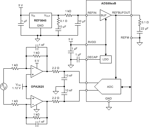 Figure 105. Differential-Input DAQ Circuit for Lowest Distortion and Noise Using the ADS890xB
8.2.1.1 Design Requirements
For this example, the design parameters are listed in Table 21.
Table 21. Design Parameters
| DESIGN PARAMETER | EXAMPLE VALUE |
|---|---|
| ADC sample rate | Maximum-specified throughput |
| Input signal | 2-kHz input, 4.5-VPP fully differential |
| Noise performance, SNR | > 101-dB, |
| Distortion, THD | < –120-dB |
| Linearity, INL | < ±2-ppm |
| Reference | 4.5 V |
| Power supply | < 5.5-V analog, 3.3-V I/O |
8.2.1.2 Detailed Design Procedure
The application circuit is illustrated in Figure 105. For simplicity, power-supply decoupling capacitors are not shown in these circuit diagrams; see the Power-Supply Recommendations section for suggested guidelines.
The reference voltage of 4.5 V is generated by the high-precision, low-noise REF5045 circuit. The output broadband noise of the reference is heavily filtered by a low-pass filter with a 3-dB cutoff frequency of 16 Hz.
Generally, the distortion from the input driver must be at least 10 dB less than the ADC distortion. The low-power OPA2625 (a high-bandwidth, low-distortion, high-precision amplifier in an inverting gain configuration) as an input driver provides exceptional ac performance because of its extremely low-distortion and high-bandwidth specifications. The distortion resulting from variation in the common-mode signal is eliminated by using the OPA2625 in an inverting gain configuration. To exercise the complete dynamic range of the device, the common-mode voltage at the ADS890xB inputs is established at a value of 2.25 V (4.5 V / 2) by using the noninverting pins of the OPA2625 amplifiers. In addition, the components of the charge kickback filter keep the noise from the front-end circuit low without adding distortion to the input signal.
For a complete schematic, see the ADS8900BEVM-PDK user's guide located in the ADS8900B SAR Analog to Digital Converter Evaluation Module web folder at www.ti.com.
The same circuit is used in reference design TIPD211, a step-by-step process to design a 20-Bit, 1-MSPS, 4-Ch Small Form Factor Design for Test and Measurement Applications using four ADS8900B SAR ADCs, four OPA2625 precision amplifiers and one REF5050 precision reference.
 |
For step-by-step design procedure, circuit schematics, bill of materials, PCB files, simulation results, and test results, refer to TI Precision Design TIPD211, 18-Bit, 1-MSPS, 4-Ch Small Form Factor Design for Test and Measurement Applications (TIDUBW7). |
8.2.1.3 Application Curves
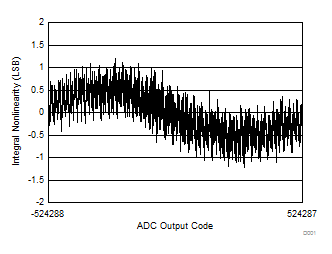
| 18-bit NMC DNL, ±1.5-ppm INL |
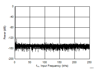
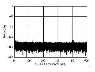
| fIN = 2 kHz, 101.8-dB SNR, –122-dB THD |
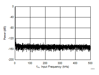
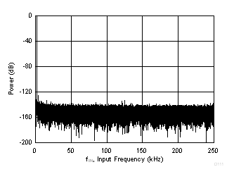
| fIN = 2 kHz, 101.8-dB SNR, –122-dB THD |
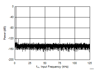
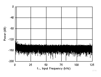
| fIN = 2 kHz, 101.8-dB SNR, –122-dB THD |
8.2.2 DAQ Circuit With FDA Input Driver and Single-Ended or Differential Input
8.2.3 Design Requirements
For this example, the design parameters are listed in Table 22.
Table 22. Design Parameters
| DESIGN PARAMETER | EXAMPLE VALUE |
|---|---|
| ADC sample rate | Maximum-specified throughput |
| Input signal | 2-kHz input, ±4.5-VPP fully differential and ±4.5-VPP single-ended bipolar signal |
| Noise performance, SNR | > 101-dB |
| Distortion, THD | < –125-dB |
| Linearity, INL | < ±2-ppm |
| Reference | 4.5 V |
| Power supply | < 5.4-V analog, 3.3-V I/O |
8.2.4 Detailed Design Procedure
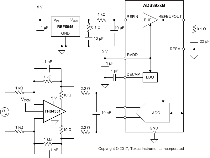
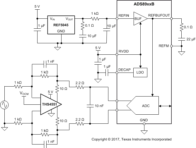
The application circuits are shown in Figure 110 and Figure 111. In both applications, the input signal is processed through a high-bandwidth, low-distortion, fully-differential amplifier (FDA) designed in a gain of 1 V/V and a low-pass RC filter before going to the ADC.
The reference voltage of 4.5 V generated by the high-precision, low-noise REF5045 circuit. The output broadband noise of the reference is heavily filtered by a low-pass filter with a 3-dB cutoff frequency of 16 Hz.
Generally, the distortion from the input driver must be at least 10 dB less than the ADC distortion. The distortion resulting from variation in the common-mode signal is eliminated by using the FDA in an inverting gain configuration that establishes a fixed common-mode level for the circuit. This configuration also eliminates the requirement of a rail-to-rail swing at the amplifier input. Therefore, these circuits use the low-power THS4551 as an input driver that provides exceptional ac performance because of its extremely low-distortion and high bandwidth specifications. In addition, the components of the charge kickback filter keep the noise from the front-end circuit low without adding distortion to the input signal.
The circuit in Figure 110 shows a fully-differential data acquisition (DAQ) block optimized for low distortion and noise using the THS4551 and ADS890xB. This front-end circuit configuration requires a differential signal at the input of the FDA and provides a differential output to drive the ADC inputs. The common-mode voltage of the input signal provided to the ADC is set by the VOCM pin of the THS4551 (not shown in Figure 110). To use the complete dynamic range of the ADC, VOCM can be set to VREF / 2 by using a simple resistive divider.
The circuit in Figure 111 shows a single-ended to differential DAQ block optimized for low distortion and noise using the THS4551 and the ADS890xB. This front-end circuit configuration requires a single-ended bipolar signal at the input of the FDA and provides a fully-differential output to drive the ADC inputs. The common-mode voltage of the input signal provided to the ADC is set by the VOCM pin of the THS4551 (not shown in Figure 111). To use the complete dynamic range of the ADC, VOCM can be set to VREF / 2 by using a simple resistive divider.
8.2.5 Application Curves
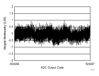
| 20-bit NMC DNL, ±1.5-ppm INL |
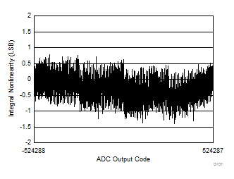
| 20-bit NMC DNL, ±1.5-ppm INL |

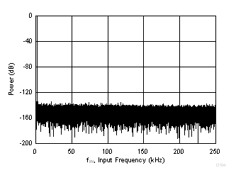
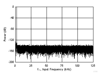
| fIN = 2 kHz, 102.1-dB SNR, –131.5-dB THD |
