JAJSCA2B June 2016 – January 2018 ADS8910B , ADS8912B , ADS8914B
PRODUCTION DATA.
- 1 特長
- 2 アプリケーション
- 3 概要
- 4 改訂履歴
- 5 Pin Configuration and Functions
- 6 Specifications
-
7 Detailed Description
- 7.1 Overview
- 7.2 Functional Block Diagram
- 7.3 Feature Description
- 7.4 Device Functional Modes
- 7.5
Programming
- 7.5.1 Output Data Word
- 7.5.2 Data Transfer Frame
- 7.5.3 Interleaving Conversion Cycles and Data Transfer Frames
- 7.5.4 Data Transfer Protocols
- 7.5.5 Device Setup
- 7.6
Register Maps
- 7.6.1
Device Configuration and Register Maps
- 7.6.1.1 PD_CNTL Register (address = 04h) [reset = 00h]
- 7.6.1.2 SDI_CNTL Register (address = 008h) [reset = 00h]
- 7.6.1.3 SDO_CNTL Register (address = 0Ch) [reset = 00h]
- 7.6.1.4 DATA_CNTL Register (address = 010h) [reset = 00h]
- 7.6.1.5 PATN_LSB Register (address = 014h) [reset = 00h]
- 7.6.1.6 PATN_MID Register (address = 015h) [reset = 00h]
- 7.6.1.7 PATN_MSB Register (address = 016h) [reset = 00h]
- 7.6.1.8 OFST_CAL Register (address = 020h) [reset = 00h]
- 7.6.1.9 REF_MRG Register (address = 030h) [reset = 00h]
- 7.6.1
Device Configuration and Register Maps
-
8 Application and Implementation
- 8.1 Application Information
- 8.2 Typical Application
- 9 Power-Supply Recommendations
- 10Layout
- 11デバイスおよびドキュメントのサポート
- 12メカニカル、パッケージ、および注文情報
パッケージ・オプション
メカニカル・データ(パッケージ|ピン)
- RGE|24
サーマルパッド・メカニカル・データ
- RGE|24
発注情報
7.3.2 Reference Buffer Module
On the CONVST rising edge, the device moves from ACQ state to CONV state, and the internal capacitors are switched to the REFBUFOUT pins as per the successive approximation algorithm. Most of the switching charge required during the conversion process is provided by external decoupling capacitor CREFBUF. If the charge lost from the CREFBUF is not replenished before the next CONVST rising edge, the voltage on REFBUFOUT pins is less than VREFBUFOUT. The subsequent conversion occurs with this different reference voltage, and causes a proportional error in the output code. The internal reference buffer of the device maintains the voltage on REFBUFOUT pins within 0.5-LSB of VREFBUFOUT. All the performance characteristics of the device are specified with the internal reference buffer and specified values of CREFBUF and RESR.
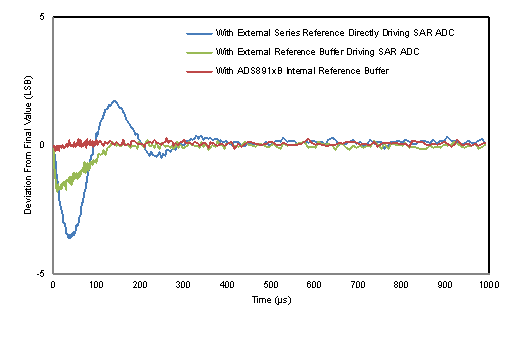
In burst-mode of operation, the device stays in ACQ state for a long duration of time and then performs a burst of conversions. During the acquisition state (ACQ), the sampling capacitor (CS) is connected to the differential input pins and no charge is drawn from the REFBUFOUT pins. However, during the very first conversion cycle, there is a step change in the current drawn from the REFBUFOUT pins. This sudden change in load triggers a transient settling response in the reference buffer. For a fixed input voltage, any transient settling error at the end of the conversion cycle results in a change in output codes over the subsequent conversions, as shown in Figure 31. The internal reference buffer of the ADS89xxB, when used with the recommended values of CREFBUF and RESR, keeps the transient settling error at the end of each conversion cycle within 0.5-LSB. Therefore, the device supports burst-mode of operation with every conversion result being as per the datasheet specifications.
 Figure 31. ADC Output Codes in Burst-Mode Operation With Various ADC Reference Buffers
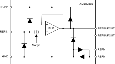
Figure 32 shows the block diagram of the internal reference buffer.
 Figure 32. Internal Reference Buffer Block Diagram
The input range for the device is set by the external voltage applied at the REFIN pin (VREF). The REFIN pin has electrostatic discharge (ESD) protection diodes to the RVDD and GND pins. For minimum input offset error (see E(IO) specified in the Electrical Characteristics), set the REF_SEL[2:0] bits to the value closest to VREF (see the OFST_CAL register).
The internal reference buffer has a typical gain of 1 V/V with minimal offset error (see V(RO) specified in the Electrical Characteristics), and the output of the buffer is available between the REFBUFOUT pins and the REFM pins. Set the REF_OFST[4:0] bits to add or subtract an intentional offset voltage (see the REF_MRG register).
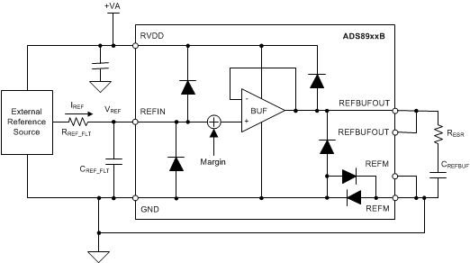
Figure 33 shows the external connections required for the internal reference buffer.
 Figure 33. External Connections for the Internal Reference Buffer
Select RREF_FLT and CREF_FLT to limit the broadband noise contribution from the external reference source. The device takes very little current, IREF, from the REFIN pin (typically, 0.1 µA). However, this current flows through RREF_FLT and may result in additional gain error.
Short the two REFBUFOUT pins externally. Short the two REFM pins to GND externally. As shown in Figure 33, place a combination of RESR and CREFBUF (see the Electrical Characteristics) between the REFBUFOUT pins and the REFM pins as close to the device as possible. See the Layout section for layout recommendations.