JAJSCA2B June 2016 – January 2018 ADS8910B , ADS8912B , ADS8914B
PRODUCTION DATA.
- 1 特長
- 2 アプリケーション
- 3 概要
- 4 改訂履歴
- 5 Pin Configuration and Functions
- 6 Specifications
-
7 Detailed Description
- 7.1 Overview
- 7.2 Functional Block Diagram
- 7.3 Feature Description
- 7.4 Device Functional Modes
- 7.5
Programming
- 7.5.1 Output Data Word
- 7.5.2 Data Transfer Frame
- 7.5.3 Interleaving Conversion Cycles and Data Transfer Frames
- 7.5.4 Data Transfer Protocols
- 7.5.5 Device Setup
- 7.6
Register Maps
- 7.6.1
Device Configuration and Register Maps
- 7.6.1.1 PD_CNTL Register (address = 04h) [reset = 00h]
- 7.6.1.2 SDI_CNTL Register (address = 008h) [reset = 00h]
- 7.6.1.3 SDO_CNTL Register (address = 0Ch) [reset = 00h]
- 7.6.1.4 DATA_CNTL Register (address = 010h) [reset = 00h]
- 7.6.1.5 PATN_LSB Register (address = 014h) [reset = 00h]
- 7.6.1.6 PATN_MID Register (address = 015h) [reset = 00h]
- 7.6.1.7 PATN_MSB Register (address = 016h) [reset = 00h]
- 7.6.1.8 OFST_CAL Register (address = 020h) [reset = 00h]
- 7.6.1.9 REF_MRG Register (address = 030h) [reset = 00h]
- 7.6.1
Device Configuration and Register Maps
-
8 Application and Implementation
- 8.1 Application Information
- 8.2 Typical Application
- 9 Power-Supply Recommendations
- 10Layout
- 11デバイスおよびドキュメントのサポート
- 12メカニカル、パッケージ、および注文情報
パッケージ・オプション
メカニカル・データ(パッケージ|ピン)
- RGE|24
サーマルパッド・メカニカル・データ
- RGE|24
発注情報
7.5.4.2.3.3 Output Data Rate Options With SRC Protocols
The device provides an option to transfer the data to the host controller at a single data rate (default, SDR) or at a double data rate (DDR). Set the DATA_RATE bit in the SDO_CNTL register to select the data transfer rate.
In SDR mode (DATA_RATE = 0b), the RVS pin toggles from low to high, and the output data bits are launched on the SDO pins on the output clock rising edge.
In DDR mode (DTA_RATE = 1b), the RVS pin toggles (from low-to-high or high-to-low), and the output data bits are launched on the SDO pins on every output clock edge, starting with the first rising edge.
The device supports all 24 combinations of output clock source, bus width, and output data rate, as shown in Table 9.
Table 9. SRC Protocol Combinations
| PROTOCOL | OUTPUT CLOCK SOURCE | BUS WIDTH | OUTPUT DATA RATE | SDI_CNTL | SDO_CNTL | #OUTPUT CLOCK
(Optimal Read Frame) |
TIMING DIAGRAM |
|---|---|---|---|---|---|---|---|
| SRC-EXT-SS | SCLK(1) | Single | SDR | 00h, 01h,
02h, or 03h(2) |
03h | 9 | Figure 73 |
| SRC-INT-SS | INTCLK(3) | Single | SDR | 43h | 9 | Figure 74 | |
| SRC-IB2-SS | INTCLK / 2(3) | Single | SDR | 83h | 9 | ||
| SRC-IB4-SS | INTCLK / 4(3) | Single | SDR | C3h | 9 | ||
| SRC-EXT-DS | SCLK(1) | Dual | SDR | 0Bh | 9 | Figure 77 | |
| SRC-INT-DS | INTCLK(3) | Dual | SDR | 4Bh | 9 | Figure 78 | |
| SRC-IB2-DS | INTCLK / 2(3) | Dual | SDR | 8Bh | 9 | ||
| SRC-IB4-DS | INTCLK / 4(3) | Dual | SDR | CBh | 9 | ||
| SRC-EXT-QS | SCLK(1) | Quad | SDR | 0Fh | 5 | Figure 81 | |
| SRC-INT-QS | INTCLK(3) | Quad | SDR | 4Fh | 5 | Figure 82 | |
| SRC-IB2-QS | INTCLK / 2(3) | Quad | SDR | 8Fh | 5 | ||
| SRC-IB4-QS | INTCLK / 4(3) | Quad | SDR | CFh | 5 | ||
| SRC-EXT-SD | SCLK(1) | Single | DDR | 13h | 9 | Figure 75 | |
| SRC-INT-SD | INTCLK(3) | Single | DDR | 53h | 9 | Figure 76 | |
| SRC-IB2-SD | INTCLK / 2(3) | Single | DDR | 93h | 9 | ||
| SRC-IB4-SD | INTCLK / 4(3) | Single | DDR | D3h | 9 | ||
| SRC-EXT-DD | SCLK(1) | Dual | DDR | 1Bh | 5 | Figure 79 | |
| SRC-INT-DD | INTCLK(3) | Dual | DDR | 5Bh | 5 | Figure 80 | |
| SRC-IB2-DD | INTCLK / 2(3) | Dual | DDR | 9Bh | 5 | ||
| SRC-IB4-DD | INTCLK / 4(3) | Dual | DDR | DBh | 5 | ||
| SRC-EXT-QD | SCLK(1) | Quad | DDR | 1Fh | 3 | Figure 83 | |
| SRC-INT-QD | INTCLK(3) | Quad | DDR | 5Fh | 3 | Figure 84 | |
| SRC-IB2-QD | INTCLK / 2(3) | Quad | DDR | 9Fh | 3 | ||
| SRC-IB4-QD | INTCLK / 4(3) | Quad | DDR | DFh | 3 |
Figure 73 to Figure 84 show the details of various source synchronous protocols. Table 9 shows the number of output clocks required in an optimal read frame for the different output protocol selections.
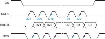 Figure 73. SRC-EXT-SS: SRC, SCLK, Single SDO, SDR
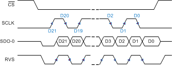 Figure 75. SRC-EXT-SD: SRC, SCLK, Single SDO, DDR
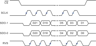 Figure 77. SRC-EXT-DS: SRC, SCLK, Dual SDO, SDR
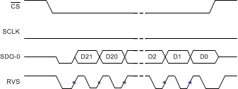 Figure 74. SRC-INT-SS: SRC, INTCLK, Single SDO, SDR
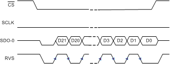 Figure 76. SRC-INT-SD: SRC, INTCLK, Single SDO, DDR
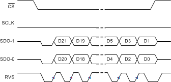 Figure 78. SRC-INT-DS: SRC, INTCLK, Dual SDO, SDR
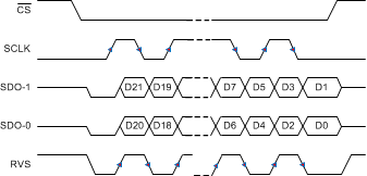 Figure 79. SRC-EXT-DD: SRC, SCLK, Dual SDO, DDR
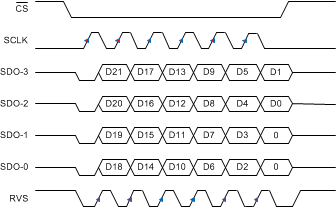 Figure 81. SRC-EXT-QS: SRC, SCLK, Quad SDO, SDR
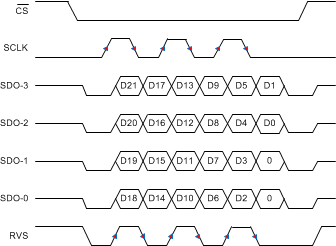 Figure 83. SRC-EXT-QD: SRC, SCLK, Quad SDO, DDR
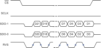 Figure 80. SRC-INT-DD: SRC, INTCLK, Dual SDO, DDR
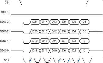 Figure 82. SRC-INT-QS: SRC, INTCLK, Quad SDO, SDR
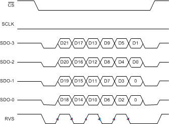 Figure 84. SRC-INT-QD: SRC, INTCLK, Quad SDO, DDR