SLOS729D October 2011 – November 2015 AFE5808A
PRODUCTION DATA.
- 1 Features
- 2 Applications
- 3 Description
- 4 Revision History
- 5 Description (continued)
- 6 Pin Configuration and Functions
- 7 Specifications
-
8 Detailed Description
- 8.1 Overview
- 8.2 Functional Block Diagram
- 8.3 Feature Description
- 8.4 Device Functional Modes
- 8.5 Programming
- 8.6
Register Maps
- 8.6.1 ADC Register Map
- 8.6.2
ADC Register/Digital Processing Description
- 8.6.2.1 AVERAGING_ENABLE: Address: 2[11]
- 8.6.2.2 ADC_OUTPUT_FORMAT: Address: 4[3]
- 8.6.2.3 DIGITAL_GAIN_ENABLE: Address: 3[12]
- 8.6.2.4 DIGITAL_HPF_ENABLE
- 8.6.2.5 DIGITAL_HPF_FILTER_K_CHX
- 8.6.2.6 LOW_FREQUENCY_NOISE_SUPPRESSION: Address: 1[11]
- 8.6.2.7 LVDS_OUTPUT_RATE_2X: Address: 1[14]
- 8.6.2.8 CHANNEL_OFFSET_SUBSTRACTION_ENABLE: Address: 3[8]
- 8.6.2.9 SERIALIZED_DATA_RATE: Address: 3[14:13]
- 8.6.2.10 TEST_PATTERN_MODES: Address: 2[15:13]
- 8.6.2.11 SYNC_PATTERN: Address: 10[8]
- 8.6.3 VCA Register Map
- 8.6.4 AFE5808A VCA Register Description
-
9 Application and Implementation
- 9.1 Application Information
- 9.2 Typical Application
- 9.3
Do's and Don'ts
- 9.3.1 Driving the Inputs (Analog or Digital) Beyond the Power-Supply Rails
- 9.3.2 Driving the Device Signal Input With an Excessively High Level Signal
- 9.3.3 Driving the VCNTL Signal With an Excessive Noise Source
- 9.3.4 Using a Clock Source With Excessive Jitter, an Excessively Long Input Clock Signal Trace, or Having Other Signals Coupled to the ADC or CW Clock Signal Trace
- 9.3.5 LVDS Routing Length Mismatch
- 9.3.6 Failure to Provide Adequate Heat Removal
- 10Power Supply Recommendations
- 11Layout
- 12Device and Documentation Support
- 13Mechanical, Packaging, and Orderable Information
1 Features
-
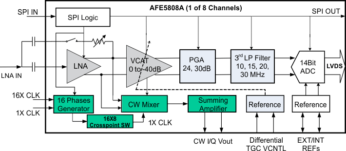
8-Channel Complete Analog Front-End
- LNA, VCAT, PGA, LPF, ADC, and CW Mixer
- Programmable Gain Low-Noise Amplifier (LNA)
- 24-, 18-, or 12-dB Gain
- 0.25-, 0.5-, or 1-VPP Linear Input Range
- 0.63-, 0.7-, or 0.9-nV/√Hz Input-Referred Noise
- Programmable Active Termination
- 40-dB, Low-Noise Voltage-Controlled Attenuator (VCAT)
- 24-, or 30-dB Programmable Gain Amplifier (PGA)
- 3rd-Order, Linear-Phase, Low-Pass Filter (LPF)
- 10 MHz, 15 MHz, 20 MHz, or 30 MHz
- 14-bit Analog-to-Digital Converter (ADC)
- 77-dBFS SNR at 65 MSPS
- LVDS Outputs
- Noise and Power Optimizations (Full Chain)
- 158 mW/CH at 0.75 nV/√Hz, 65 MSPS
- 101 mW/CH at 1.1 nV/√Hz, 40 MSPS
- 80 mW/CH in CW Mode
- Excellent Device-to-Device Gain Matching
- ±0.5 dB (Typical) and ±0.9 dB (Maximum)
- Low Harmonic Distortion
- Fast and Consistent Overload Recovery
- Passive Mixer for Continuous Wave Doppler (CWD)
- Low Close-in Phase Noise: –156 dBc/Hz at 1 KHz Off 2.5-MHz Carrier
- Phase Resolution of 1/16λ
- Support 16X, 8X, 4X and 1X CW Clocks
- 12-dB Suppression on 3rd and 5th Harmonics
- Flexible Input Clocks
- Small Package: 15-mm × 9-mm, 135-Pin NFBGA
2 Applications
- Medical Ultrasound Imaging
- Nondestructive Evaluation Equipments
3 Description
The AFE5808A is a highly-integrated, analog front-end (AFE) solution specifically designed for ultrasound systems in which high performance and small size are required. The AFE5808A integrates a complete time-gain-control (TGC) imaging path and a continuous wave Doppler (CWD) path. This device also enables users to select one of various power and noise combinations to optimize system performance. Therefore, the AFE5808A is an outstanding ultrasound analog front-end solution not only for high-end systems, but also for portable ones.
Device Information(1)
| PART NUMBER | PACKAGE | BODY SIZE (NOM) |
|---|---|---|
| AFE5808A | NFBGA (135) | 9.00 mm × 15.00 mm |
- For all available packages, see the package option addendum at the end of the data sheet.
Block Diagram
