JAJSDZ0J October 2011 – April 2016 AM3351 , AM3352 , AM3354 , AM3356 , AM3357 , AM3358 , AM3359
PRODUCTION DATA.
- 1デバイスの概要
- 2改訂履歴
- 3Device Comparison
- 4Terminal Configuration and Functions
-
5Specifications
- 5.1 Absolute Maximum Ratings
- 5.2 ESD Ratings
- 5.3 Power-On Hours (POH)
- 5.4 Operating Performance Points (OPPs)
- 5.5 Recommended Operating Conditions
- 5.6 Power Consumption Summary
- 5.7 DC Electrical Characteristics
- 5.8 Thermal Resistance Characteristics for ZCE and ZCZ Packages
- 5.9 External Capacitors
- 5.10 Touch Screen Controller and Analog-to-Digital Subsystem Electrical Parameters
- 6Power and Clocking
-
7Peripheral Information and Timings
- 7.1 Parameter Information
- 7.2 Recommended Clock and Control Signal Transition Behavior
- 7.3 OPP50 Support
- 7.4 Controller Area Network (CAN)
- 7.5 DMTimer
- 7.6 Ethernet Media Access Controller (EMAC) and Switch
- 7.7
External Memory Interfaces
- 7.7.1 General-Purpose Memory Controller (GPMC)
- 7.7.2
mDDR(LPDDR), DDR2, DDR3, DDR3L Memory Interface
- 7.7.2.1 mDDR (LPDDR) Routing Guidelines
- 7.7.2.2
DDR2 Routing Guidelines
- 7.7.2.2.1 Board Designs
- 7.7.2.2.2
DDR2 Interface
- 7.7.2.2.2.1 DDR2 Interface Schematic
- 7.7.2.2.2.2 Compatible JEDEC DDR2 Devices
- 7.7.2.2.2.3 PCB Stackup
- 7.7.2.2.2.4 Placement
- 7.7.2.2.2.5 DDR2 Keepout Region
- 7.7.2.2.2.6 Bulk Bypass Capacitors
- 7.7.2.2.2.7 High-Speed (HS) Bypass Capacitors
- 7.7.2.2.2.8 Net Classes
- 7.7.2.2.2.9 DDR2 Signal Termination
- 7.7.2.2.2.10 DDR_VREF Routing
- 7.7.2.2.3 DDR2 CK and ADDR_CTRL Routing
- 7.7.2.3
DDR3 and DDR3L Routing Guidelines
- 7.7.2.3.1 Board Designs
- 7.7.2.3.2 DDR3 Device Combinations
- 7.7.2.3.3
DDR3 Interface
- 7.7.2.3.3.1 DDR3 Interface Schematic
- 7.7.2.3.3.2 Compatible JEDEC DDR3 Devices
- 7.7.2.3.3.3 PCB Stackup
- 7.7.2.3.3.4 Placement
- 7.7.2.3.3.5 DDR3 Keepout Region
- 7.7.2.3.3.6 Bulk Bypass Capacitors
- 7.7.2.3.3.7 High-Speed Bypass Capacitors
- 7.7.2.3.3.8 Net Classes
- 7.7.2.3.3.9 DDR3 Signal Termination
- 7.7.2.3.3.10 DDR_VREF Routing
- 7.7.2.3.3.11 VTT
- 7.7.2.3.4 DDR3 CK and ADDR_CTRL Topologies and Routing Definition
- 7.7.2.3.5 Data Topologies and Routing Definition
- 7.7.2.3.6 Routing Specification
- 7.8 I2C
- 7.9 JTAG Electrical Data and Timing
- 7.10 LCD Controller (LCDC)
- 7.11 Multichannel Audio Serial Port (McASP)
- 7.12 Multichannel Serial Port Interface (McSPI)
- 7.13 Multimedia Card (MMC) Interface
- 7.14 Programmable Real-Time Unit Subsystem and Industrial Communication Subsystem (PRU-ICSS)
- 7.15 Universal Asynchronous Receiver Transmitter (UART)
- 8Device and Documentation Support
- 9Mechanical, Packaging, and Orderable Information
パッケージ・オプション
デバイスごとのパッケージ図は、PDF版データシートをご参照ください。
メカニカル・データ(パッケージ|ピン)
- ZCZ|324
サーマルパッド・メカニカル・データ
発注情報
6 Power and Clocking
6.1 Power Supplies
6.1.1 Power Supply Slew Rate Requirement
To maintain the safe operating range of the internal ESD protection devices, TI recommends limiting the maximum slew rate for powering on the supplies to be less than 1.0E +5 V/s. For instance, as shown in Figure 6-1, TI recommends a value greater than 18 µs for the supply ramp slew for a 1.8-V supply.
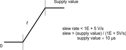 Figure 6-1 Power Supply Slew and Slew Rate
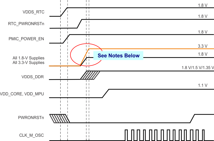
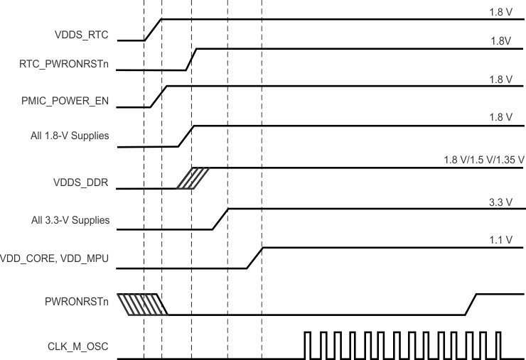
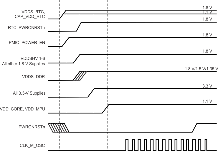
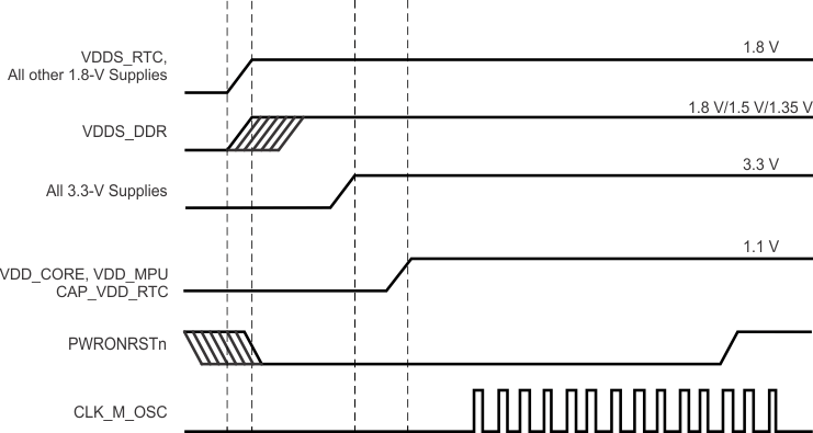
6.1.2 Power-Down Sequencing
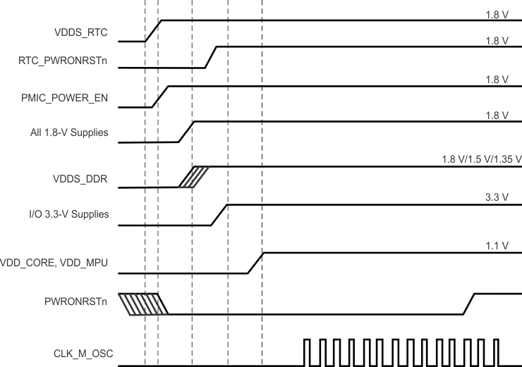
PWRONRSTn input terminal should be taken low, which stops all internal clocks before power supplies are turned off. All other external clocks to the device should be shut off.
The preferred way to sequence power down is to have all the power supplies ramped down sequentially in the exact reverse order of the power-up sequencing. In other words, the power supply that has been ramped up first should be the last one that should be ramped down. This ensures there would be no spurious current paths during the power-down sequence. The VDDS power supply must ramp down after all 3.3-V VDDSHVx [1-6] power supplies.
If it is desired to ramp down VDDS and VDDSHVx [1-6] simultaneously, it should always be ensured that the difference between VDDS and VDDSHVx [1-6] during the entire power-down sequence is <2 V. Any violation of this could cause reliability risks for the device. TI recommends maintaining VDDS ≥1.5V as all the other supplies fully ramp down to minimize in-rush currents.
If none of the VDDSHVx [1-6] power supplies are configured as 3.3 V, the VDDS power supply may ramp down along with the VDDSHVx [1-6] supplies or after all the VDDSHVx [1-6] supplies have ramped down. TI recommends maintaining VDDS ≥1.5V as all the other supplies fully ramp down to minimize in-rush currents.
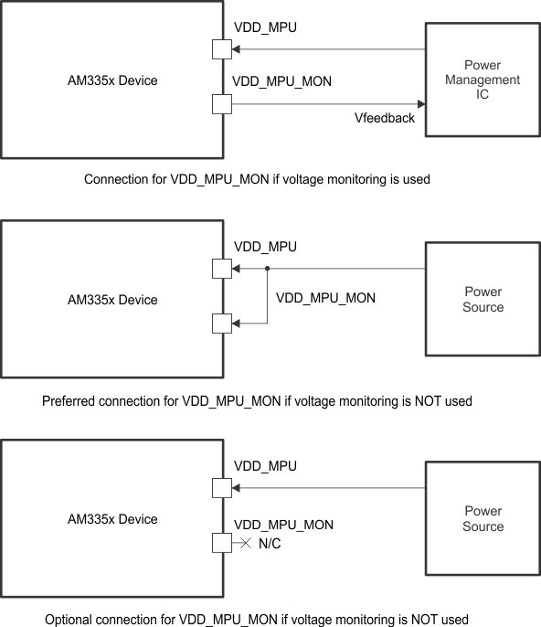
6.1.3 VDD_MPU_MON Connections
Figure 6-7 shows the VDD_MPU_MON connectivity. VDD_MPU_MON connectivity is available only on the ZCZ package.
6.1.4 Digital Phase-Locked Loop Power Supply Requirements
The digital phase-locked loop (DPLL) provides all interface clocks and functional clocks to the processor of the AM335x device. The AM335x device integrates five different DPLLs—Core DPLL, Per DPLL, LCD DPLL, DDR DPLL, MPU DPLL.
Figure 6-8 shows the power supply connectivity implemented in the AM335x device. Table 6-1 provides the power supply requirements for the DPLL.
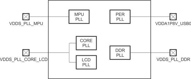 Figure 6-8 DPLL Power Supply Connectivity
Table 6-1 DPLL Power Supply Requirements
| SUPPLY NAME | DESCRIPTION | MIN | NOM | MAX | UNIT |
|---|---|---|---|---|---|
| VDDA1P8V_USB0 | Supply voltage range for USBPHY and PER DPLL, Analog, 1.8 V | 1.71 | 1.8 | 1.89 | V |
| Max peak-to-peak supply noise | 50 | mV (p-p) | |||
| VDDS_PLL_MPU | Supply voltage range for DPLL MPU, analog | 1.71 | 1.8 | 1.89 | V |
| Max peak-to-peak supply noise | 50 | mV (p-p) | |||
| VDDS_PLL_CORE_LCD | Supply voltage range for DPLL CORE and LCD, analog | 1.71 | 1.8 | 1.89 | V |
| Max peak-to-peak supply noise | 50 | mV (p-p) | |||
| VDDS_PLL_DDR | Supply voltage range for DPLL DDR, analog | 1.71 | 1.8 | 1.89 | V |
| Max peak-to-peak supply noise | 50 | mV (p-p) |
6.2 Clock Specifications
6.2.1 Input Clock Specifications
The AM335x device has two clock inputs. Each clock input passes through an internal oscillator which can be connected to an external crystal circuit (oscillator mode) or external LVCMOS square-wave digital clock source (bypass mode). The oscillators automatically operate in bypass mode when their input is connected to an external LVCMOS square-wave digital clock source. The oscillator associated with a specific clock input must be enabled when the clock input is being used in either oscillator mode or bypass mode.
The OSC1 oscillator provides a 32.768-kHz reference clock to the real-time clock (RTC) and is connected to the RTC_XTALIN and RTC_XTALOUT terminals. This clock source is referred to as the 32K oscillator (CLK_32K_RTC) in the AM335x and AMIC110 Sitara Processors Technical Reference Manual. OSC1 is disabled by default after power is applied. This clock input is optional and may not be required if the RTC is configured to receive a clock from the internal 32k RC oscillator (CLK_RC32K) or peripheral PLL (CLK_32KHZ) which receives a reference clock from the OSC0 input.
The OSC0 oscillator provides a 19.2-MHz, 24-MHz, 25-MHz, or 26-MHz reference clock which is used to clock all non-RTC functions and is connected to the XTALIN and XTALOUT terminals. This clock source is referred to as the master oscillator (CLK_M_OSC) in the AM335x and AMIC110 Sitara Processors Technical Reference Manual. OSC0 is enabled by default after power is applied.
For more information related to recommended circuit topologies and crystal oscillator circuit requirements for these clock inputs, see Section 6.2.2.
6.2.2 Input Clock Requirements
6.2.2.1 OSC0 Internal Oscillator Clock Source
Figure 6-9 shows the recommended crystal circuit. TI recommends that preproduction printed-circuit board (PCB) designs include the two optional resistors Rbias and Rd in case they are required for proper oscillator operation when combined with production crystal circuit components. In most cases, Rbias is not required and Rd is a 0-Ω resistor. These resistors may be removed from production PCB designs after evaluating oscillator performance with production crystal circuit components installed on preproduction PCBs.
The XTALIN terminal has a 15- to 40-kΩ internal pulldown resistor which is enabled when OSC0 is disabled. This internal resistor prevents the XTALIN terminal from floating to an invalid logic level which may increase leakage current through the oscillator input buffer.
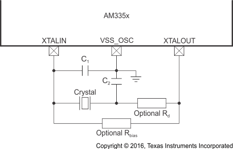
Table 6-2 OSC0 Crystal Circuit Requirements
| PARAMETER | MIN | TYP | MAX | UNIT | ||
|---|---|---|---|---|---|---|
| ƒxtal | Crystal parallel resonance frequency | Fundamental mode oscillation only | 19.2, 24, 25, or 26 | MHz | ||
| Crystal frequency stability and tolerance(1) | –50 | 50 | ppm | |||
| CC1 | C1 capacitance | Cshunt ≤ 5 pF | 12 | 24 | pF | |
| Cshunt > 5 pF | 18 | 24 | ||||
| CC2 | C2 capacitance | Cshunt ≤ 5 pF | 12 | 24 | pF | |
| Cshunt > 5 pF | 18 | 24 | ||||
| Cshunt | Shunt capacitance | 7 | pF | |||
| ESR | Crystal effective series resistance | ƒxtal = 19.2 MHz, oscillator has nominal negative resistance of 272 Ω and worst-case negative resistance of 163 Ω | 54.4 | Ω | ||
| ƒxtal = 24 MHz, oscillator has nominal negative resistance of 240 Ω and worst-case negative resistance of 144 Ω | 48.0 | |||||
| ƒxtal = 25 MHz, oscillator has nominal negative resistance of 233 Ω and worst-case negative resistance of 140 Ω | 46.6 | |||||
| ƒxtal = 26 MHz, oscillator has nominal negative resistance of 227 Ω and worst-case negative resistance of 137 Ω | 45.3 | |||||
Table 6-3 OSC0 Crystal Circuit Characteristics
| NAME | DESCRIPTION | MIN | TYP | MAX | UNIT | |
|---|---|---|---|---|---|---|
| Cpkg | Shunt capacitance of package | ZCE package | 0.01 | pF | ||
| ZCZ package | 0.01 | |||||
| Pxtal | The actual values of the ESR, ƒxtal, and CL should be used to yield a typical crystal power dissipation value. Using the maximum values specified for ESR, ƒxtal, and CL parameters yields a maximum power dissipation value. | Pxtal = 0.5 ESR (2 π ƒxtal CL VDDS_OSC)2 | ||||
| tsX | Start-up time | 1.5 | ms | |||
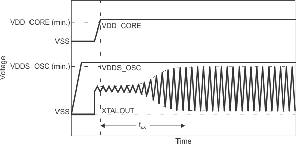 Figure 6-10 OSC0 Start-Up Time
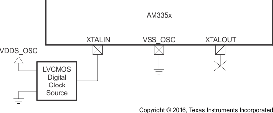
6.2.2.2 OSC0 LVCMOS Digital Clock Source
Figure 6-11 shows the recommended oscillator connections when OSC0 is connected to an LVCMOS square-wave digital clock source. The LVCMOS clock source is connected to the XTALIN terminal. The ground for the LVCMOS clock source and VSS_OSC should be connected directly to the nearest PCB digital ground (VSS). In this mode of operation, the XTALOUT terminal should not be used to source any external components. The PCB design should provide a mechanism to disconnect the XTALOUT terminal from any external components or signal traces that may couple noise into OSC0 via the XTALOUT terminal.
The XTALIN terminal has a 15- to 40-kΩ internal pulldown resistor which is enabled when OSC0 is disabled. This internal resistor prevents the XTALIN terminal from floating to an invalid logic level which may increase leakage current through the oscillator input buffer.
Table 6-4 OSC0 LVCMOS Reference Clock Requirements
| NAME | DESCRIPTION | MIN | TYP | MAX | UNIT | |
|---|---|---|---|---|---|---|
| ƒ(XTALIN) | Frequency, LVCMOS reference clock | 19.2, 24, 25, or 26 | MHz | |||
| Frequency, LVCMOS reference clock stability and tolerance(1) | –50 | 50 | ppm | |||
| tdc(XTALIN) | Duty cycle, LVCMOS reference clock period | 45% | 55% | |||
| tjpp(XTALIN) | Jitter peak-to-peak, LVCMOS reference clock period | –1% | 1% | |||
| tR(XTALIN) | Time, LVCMOS reference clock rise | 5 | ns | |||
| tF(XTALIN) | Time, LVCMOS reference clock fall | 5 | ns | |||
6.2.2.3 OSC1 Internal Oscillator Clock Source
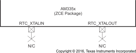
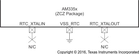
Figure 6-12 shows the recommended crystal circuit for OSC1 of the ZCE package and Figure 6-13 shows the recommended crystal circuit for OSC1 of the ZCZ package. TI recommends that preproduction PCB designs include the two optional resistors Rbias and Rd in case they are required for proper oscillator operation when combined with production crystal circuit components. In most cases, Rbias is not required and Rd is a 0-Ω resistor. These resistors may be removed from production PCB designs after evaluating oscillator performance with production crystal circuit components installed on preproduction PCBs.
The RTC_XTALIN terminal has a 10- to 40-kΩ internal pullup resistor which is enabled when OSC1 is disabled. This internal resistor prevents the RTC_XTALIN terminal from floating to an invalid logic level which may increase leakage current through the oscillator input buffer.
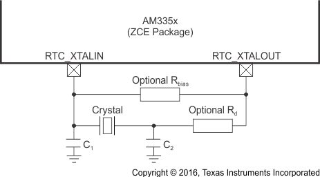
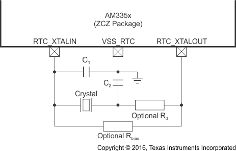
Table 6-5 OSC1 Crystal Circuit Requirements
| NAME | DESCRIPTION | MIN | TYP | MAX | UNIT | |
|---|---|---|---|---|---|---|
| ƒxtal | Crystal parallel resonance frequency | Fundamental mode oscillation only | 32.768 | kHz | ||
| Crystal frequency stability and tolerance(1) | Maximum RTC error = 10.512 minutes per year | –20.0 | 20.0 | ppm | ||
| Maximum RTC error = 26.28 minutes per year | –50.0 | 50.0 | ppm | |||
| CC1 | C1 capacitance | 12.0 | 24.0 | pF | ||
| CC2 | C2 capacitance | 12.0 | 24.0 | pF | ||
| Cshunt | Shunt capacitance | 1.5 | pF | |||
| ESR | Crystal effective series resistance | ƒxtal = 32.768 kHz, oscillator has nominal negative resistance of 725 kΩ and worst-case negative resistance of 250 kΩ | 80 | kΩ | ||
Table 6-6 OSC1 Crystal Circuit Characteristics
| NAME | DESCRIPTION | MIN | TYP | MAX | UNIT | |
|---|---|---|---|---|---|---|
| Cpkg | Shunt capacitance of package | ZCE package | 0.17 | pF | ||
| ZCZ package | 0.01 | pF | ||||
| Pxtal | The actual values of the ESR, ƒxtal, and CL should be used to yield a typical crystal power dissipation value. Using the maximum values specified for ESR, ƒxtal, and CL parameters yields a maximum power dissipation value. | Pxtal = 0.5 ESR (2 π ƒxtal CL VDDS_RTC)2 | ||||
| tsX | Start-up time | 2 | s | |||
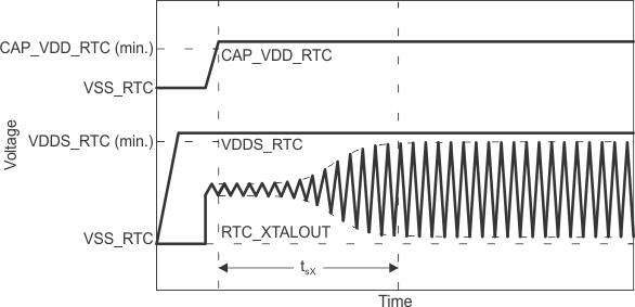 Figure 6-14 OSC1 Start-up Time
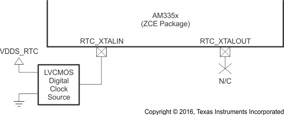
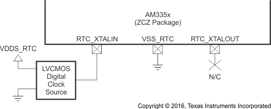
6.2.2.4 OSC1 LVCMOS Digital Clock Source
Figure 6-15 shows the recommended oscillator connections when OSC1 of the ZCE package is connected to an LVCMOS square-wave digital clock source and Figure 6-16 shows the recommended oscillator connections when OSC1 of the ZCZ package is connected to an LVCMOS square-wave digital clock source. The LVCMOS clock source is connected to the RTC_XTALIN terminal. The ground for the LVCMOS clock source and VSS_RTC of the ZCZ package should be connected directly to the nearest PCB digital ground (VSS). In this mode of operation, the RTC_XTALOUT terminal should not be used to source any external components. The PCB design should provide a mechanism to disconnect the RTC_XTALOUT terminal from any external components or signal traces that may couple noise into OSC1 through the RTC_XTALOUT terminal.
The RTC_XTALIN terminal has a 10- to 40-kΩ internal pullup resistor which is enabled when OSC1 is disabled. This internal resistor prevents the RTC_XTALIN terminal from floating to an invalid logic level which may increase leakage current through the oscillator input buffer.
Table 6-7 OSC1 LVCMOS Reference Clock Requirements
| NAME | DESCRIPTION | MIN | TYP | MAX | UNIT | |
|---|---|---|---|---|---|---|
| ƒ(RTC_XTALIN) | Frequency, LVCMOS reference clock | 32.768 | kHz | |||
| Frequency, LVCMOS reference clock stability and tolerance(1) | Maximum RTC error = 10.512 minutes/year | –20 | 20 | ppm | ||
| Maximum RTC error = 26.28 minutes/year | –50 | 50 | ppm | |||
| tdc(RTC_XTALIN) | Duty cycle, LVCMOS reference clock period | 45% | 55% | |||
| tjpp(RTC_XTALIN) | Jitter peak-to-peak, LVCMOS reference clock period | –1% | 1% | |||
| tR(RTC_XTALIN) | Time, LVCMOS reference clock rise | 5 | ns | |||
| tF(RTC_XTALIN) | Time, LVCMOS reference clock fall | 5 | ns | |||
6.2.2.5 OSC1 Not Used
Figure 6-17 shows the recommended oscillator connections when OSC1 of the ZCE package is not used and Figure 6-18 shows the recommended oscillator connections when OSC1 of the ZCZ package is not used. An internal 10-kΩ pullup on the RTC_XTALIN terminal is turned on when OSC1 is disabled to prevent this input from floating to an invalid logic level which may increase leakage current through the oscillator input buffer. OSC1 is disabled by default after power is applied. Therefore, both RTC_XTALIN and RTC_XTALOUT terminals should be a no connect (NC) when OSC1 is not used.
6.2.3 Output Clock Specifications
The AM335x device has two clock output signals. The CLKOUT1 signal is always a replica of the OSC0 input clock which is referred to as the master oscillator (CLK_M_OSC) in the AM335x and AMIC110 Sitara Processors Technical Reference Manual. The CLKOUT2 signal can be configured to output the OSC1 input clock, which is referred to as the 32K oscillator (CLK_32K_RTC) in the AM335x and AMIC110 Sitara Processors Technical Reference Manual, or four other internal clocks. For more information related to configuring these clock output signals, see the CLKOUT Signals section of the AM335x and AMIC110 Sitara Processors Technical Reference Manual.
6.2.4 Output Clock Characteristics
NOTE
The AM335x CLKOUT1 and CLKOUT2 clock outputs should not be used as a synchronous clock for any of the peripheral interfaces because they were not timing closed to any other signals. These clock outputs also were not designed to source any time critical external circuits that require a low jitter reference clock. The jitter performance of these outputs is unpredictable due to complex combinations of many system variables. For example, CLKOUT2 may be sourced from several PLLs with each PLL supporting many configurations that yield different jitter performance. There are also other unpredictable contributors to jitter performance such as application specific noise or crosstalk into the clock circuits. Therefore, there are no plans to specify jitter performance for these outputs.
6.2.4.1 CLKOUT1
The CLKOUT1 signal can be output on the XDMA_EVENT_INTR0 terminal. This terminal connects to one of seven internal signals via configurable multiplexers. The XDMA_EVENT_INTR0 multiplexer must be configured for Mode 3 to connect the CLKOUT1 signal to the XDMA_EVENT_INTR0 terminal.
The default reset configuration of the XDMA_EVENT_INTR0 multiplexer is selected by the logic level applied to the LCD_DATA5 terminal on the rising edge of PWRONRSTn. The XDMA_EVENT_INTR0 multiplexer is configured to Mode 7 if the LCD_DATA5 terminal is low on the rising edge of PWRONRSTn or Mode 3 if the LCD_DATA5 terminal is high on the rising edge of PWRONRSTn. This allows the CLKOUT1 signal to be output on the XDMA_EVENT_INTR0 terminal without software intervention. In this mode, the output is held low while PWRONRSTn is active and begins to toggle after PWRONRSTn is released.
6.2.4.2 CLKOUT2
The CLKOUT2 signal can be output on the XDMA_EVENT_INTR1 terminal. This terminal connects to one of seven internal signals via configurable multiplexers. The XDMA_EVENT_INTR1 multiplexer must be configured for Mode 3 to connect the CLKOUT2 signal to the XDMA_EVENT_INTR1 terminal.
The default reset configuration of the XDMA_EVENT_INTR1 multiplexer is always Mode 7. Software must configure the XDMA_EVENT_INTR1 multiplexer to Mode 3 for the CLKOUT2 signal to be output on the XDMA_EVENT_INTR1 terminal.
