SPRS550F October 2009 – July 2014 AM3505 , AM3517
PRODUCTION DATA.
- 1Device Summary
- 2Revision History
- 3Device Comparison
- 4Terminal Configuration and Functions
- 5Specifications
-
6Timing Requirements and Switching Characteristics
- 6.1 Timing Test Conditions
- 6.2 Interface Clock Specifications
- 6.3 Timing Parameters
- 6.4
External Memory Interfaces
- 6.4.1 General-Purpose Memory Controller (GPMC)
- 6.4.2
SDRAM Controller (SDRC)
- 6.4.2.1 LPDDR Interface
- 6.4.2.2
DDR2 Interface
- 6.4.2.2.1 DDR2 Interface Schematic
- 6.4.2.2.2 Compatible JEDEC DDR2 Devices
- 6.4.2.2.3 PCB Stackup
- 6.4.2.2.4 Placement
- 6.4.2.2.5 DDR2 Keep Out Region
- 6.4.2.2.6 Bulk Bypass Capacitors
- 6.4.2.2.7 High-Speed Bypass Capacitors
- 6.4.2.2.8 Net Classes
- 6.4.2.2.9 DDR2 Signal Termination
- 6.4.2.2.10 VREF Routing
- 6.4.2.2.11 DDR2 CLK and ADDR_CTRL Routing
- 6.4.2.2.12 On Die Termination (ODT)
- 6.5 Video Interfaces
- 6.6
Serial Communications Interfaces
- 6.6.1 Multichannel Buffered Serial Port (McBSP) Timing
- 6.6.2 Multichannel Serial Port Interface (McSPI) Timing
- 6.6.3 Multiport Full-Speed Universal Serial Bus (USB) Interface
- 6.6.4 Multiport High-Speed Universal Serial Bus (USB) Timing
- 6.6.5 USB0 OTG (USB2.0 OTG)
- 6.6.6 High-End Controller Area Network Controller (HECC) Timing
- 6.6.7 Ethernet Media Access Controller (EMAC)
- 6.6.8 Management Data Input/Output (MDIO)
- 6.6.9 Universal Asynchronous Receiver/Transmitter (UART)
- 6.6.10 HDQ / 1-Wire Interfaces
- 6.6.11 I2C Interface
- 6.7 Removable Media Interfaces
- 6.8 Test Interfaces
- 7Device and Documentation Support
- 8Mechanical Packaging and Orderable Information
パッケージ・オプション
デバイスごとのパッケージ図は、PDF版データシートをご参照ください。
メカニカル・データ(パッケージ|ピン)
- ZER|484
- ZCN|491
サーマルパッド・メカニカル・データ
発注情報
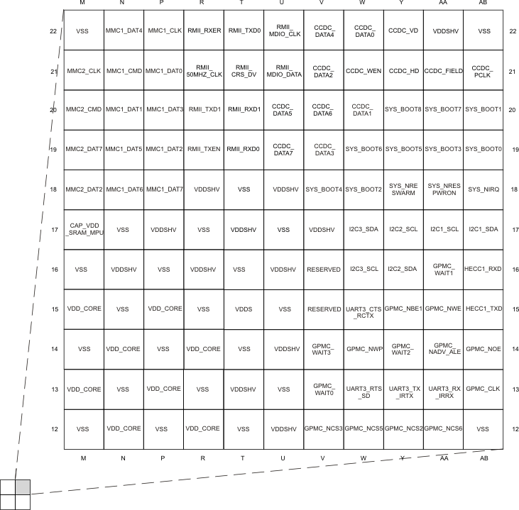
4 Terminal Configuration and Functions
4.1 Pin Assignments
4.1.1 Pin Map (Top View)
The following illustrations show the top views of the 484-pin [ZER] and 491-pin [ZCN] package pin assignments in four quadrants (A, B, C, and D).
Note: A pin with an NC designator indicates No Connection. For proper device operation, these pins must be left unconnected.
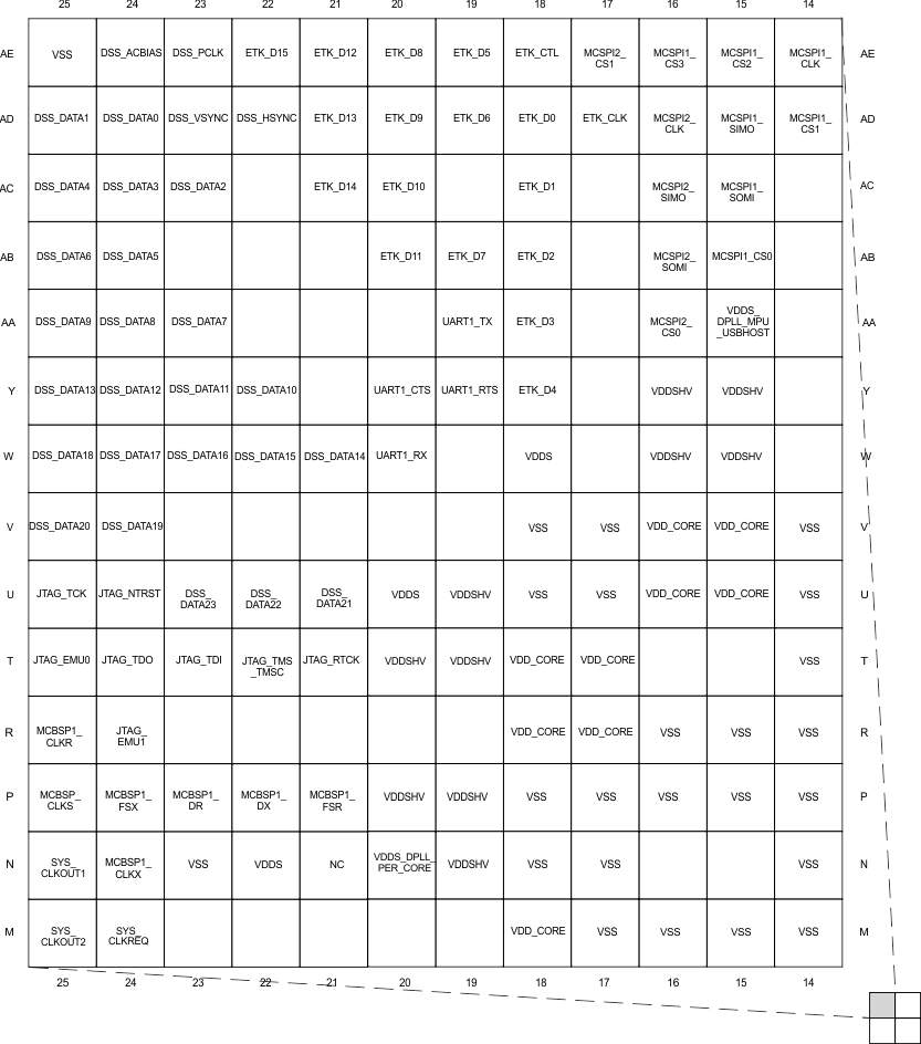 Figure 4-1 ZCN Pin Map [Quadrant A]
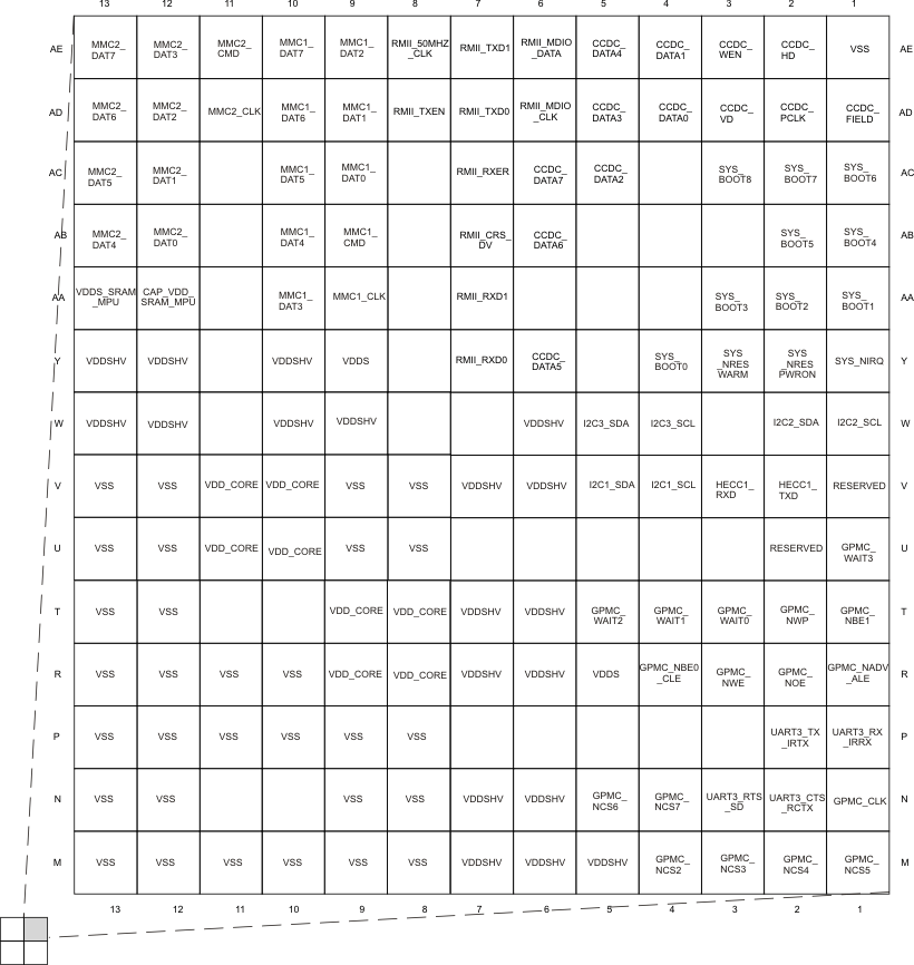 Figure 4-2 ZCN Pin Map [Quadrant B]
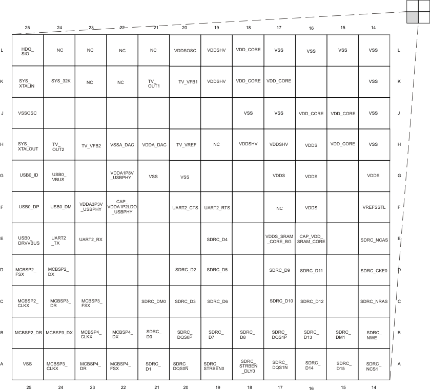 Figure 4-3 ZCN Pin Map [Quadrant C]
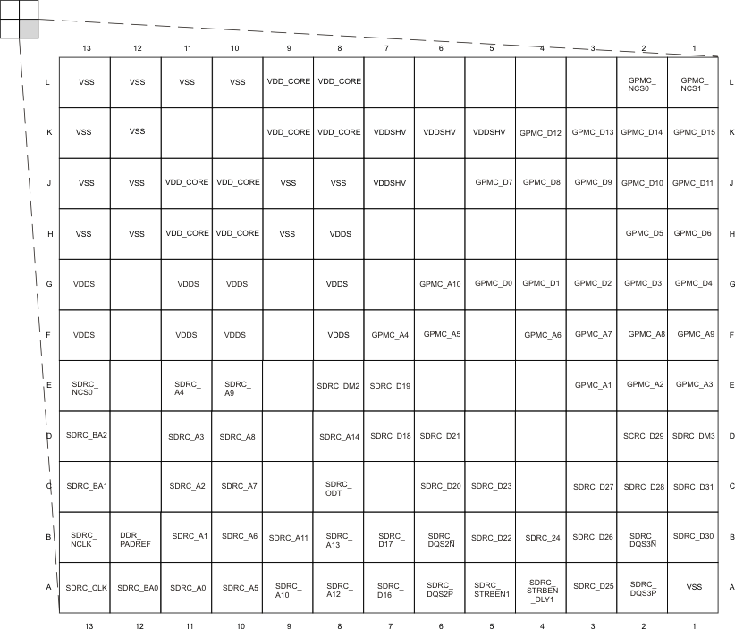 Figure 4-4 ZCN Pin Map [Quadrant D]
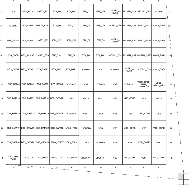 Figure 4-5 ZER Pin Map [Quadrant A]
 ZER Pin Map [Quadrant B]
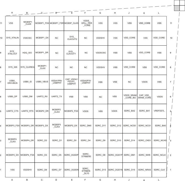 Figure 4-6 ZER Pin Map [Quadrant C]
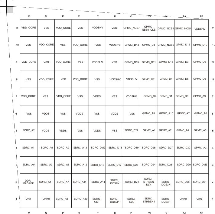 Figure 4-7 ZER Pin Map [Quadrant D]
4.2 Ball Characteristics
Table 4-1 and Table 4-2 describe the terminal characteristics and the signals multiplexed on each pin for the ZCN/ZER packages. The following list describes the table column headers.
- BALL LOCATION: Ball number(s) on the bottom side associated with each signal(s) on the bottom.
-
PIN NAME: Names of signals multiplexed on each ball (also notice that the name of the pin is the signal name in mode 0).
Note: The Ball Characteristics table does not take into account subsystem pin multiplexing options. Subsystem pin multiplexing options are described in Section 4.4, Signal Description. -
MODE: Multiplexing mode number.
- Mode 0 is the primary mode; this means that when mode 0 is set, the function mapped on the pin corresponds to the name of the pin. There is always a function mapped on the primary mode. Notice that primary mode is not necessarily the default mode.
- Modes 1 to 7 are possible modes for alternate functions. On each pin, some modes are effectively used for alternate functions, while some modes are not used and do not correspond to a functional configuration.
Note: The default mode is the mode which is automatically configured on release of the internal GLOBAL_PWRON reset; also see the RESET REL. MODE column.
-
TYPE: Signal direction
- I = Input
- O = Output
- I/O = Input/Output
- D = Open drain
- DS = Differential
- A = Analog
Note: In the safe_mode, the buffer is configured in high-impedance.
-
BALL RESET STATE: The state of the terminal at reset (power up).
- 0: The buffer drives VOL (pulldown/pullup resistor not activated)
0(PD): The buffer drives VOL with an active pulldown resistor. - 1: The buffer drives VOH (pulldown/pullup resistor not activated)
1(PU): The buffer drives VOH with an active pullup resistor. - Z: High-impedance
- L: High-impedance with an active pulldown resistor
- H: High-impedance with an active pullup resistor
- 0: The buffer drives VOL (pulldown/pullup resistor not activated)
-
BALL RESET REL. STATE: The state of the terminal at reset release.
- 0: The buffer drives VOL (pulldown/pullup resistor not activated)
0(PD): The buffer drives VOL with an active pulldown resistor. - 1: The buffer drives VOH (pulldown/pullup resistor not activated)
1(PU): The buffer drives VOH with an active pullup resistor. - Z: High-impedance
- L: High-impedance with an active pulldown resistor
- H : High-impedance with an active pullup resistor
- 0: The buffer drives VOL (pulldown/pullup resistor not activated)
- RESET REL. MODE: This mode is automatically configured on release of the internal GLOBAL_PWRON reset.
- POWER: The voltage supply that powers the terminal’s I/O buffers.
- VOLTAGE: Supply voltage for associated pin.
- HYS: Indicates if the input buffer is with hysteresis.
- LOAD: Load capacitance of the associated output buffer.
- PULL U/D - TYPE: Denotes the presence of an internal pullup or pulldown resistor. Pullup and pulldown resistors can be enabled or disabled via software.
- IO CELL: IO cell information.
Note: Configuring two pins to the same input signal is not supported as it can yield unexpected results. This can be easily prevented with the proper software configuration.
Table 4-1 Ball Characteristics (ZCN Pkg.)
| BALL LOCATION [1] | PIN NAME [2] | MODE [3] | TYPE [4] | BALL RESET STATE [5] | BALL RESET REL. STATE [6] | RESET REL. MODE [7] | POWER [8] | VOLTAGE [9] | HYS [10] | LOAD (pF) [11] | PULL U/D TYPE [12] | IO CELL [13] |
|---|---|---|---|---|---|---|---|---|---|---|---|---|
| B21 | sdrc_d0 | 0 | IO | L | Z | 0 | VDDS | 1.8V | Yes | 4 | PU/ PD | LVCMOS |
| A21 | sdrc_d1 | 0 | IO | L | Z | 0 | VDDS | 1.8V | Yes | 4 | PU/ PD | LVCMOS |
| D20 | sdrc_d2 | 0 | IO | L | Z | 0 | VDDS | 1.8V | Yes | 4 | PU/ PD | LVCMOS |
| C20 | sdrc_d3 | 0 | IO | L | Z | 0 | VDDS | 1.8V | Yes | 4 | PU/ PD | LVCMOS |
| E19 | sdrc_d4 | 0 | IO | L | Z | 0 | VDDS | 1.8V | Yes | 4 | PU/ PD | LVCMOS |
| D19 | sdrc_d5 | 0 | IO | L | Z | 0 | VDDS | 1.8V | Yes | 4 | PU/ PD | LVCMOS |
| C19 | sdrc_d6 | 0 | IO | L | Z | 0 | VDDS | 1.8V | Yes | 4 | PU/ PD | LVCMOS |
| B19 | sdrc_d7 | 0 | IO | L | Z | 0 | VDDS | 1.8V | Yes | 4 | PU/ PD | LVCMOS |
| B18 | sdrc_d8 | 0 | IO | L | Z | 0 | VDDS | 1.8V | Yes | 4 | PU/ PD | LVCMOS |
| D17 | sdrc_d9 | 0 | IO | L | Z | 0 | VDDS | 1.8V | Yes | 4 | PU/ PD | LVCMOS |
| C17 | sdrc_d10 | 0 | IO | L | Z | 0 | VDDS | 1.8V | Yes | 4 | PU/ PD | LVCMOS |
| D16 | sdrc_d11 | 0 | IO | L | Z | 0 | VDDS | 1.8V | Yes | 4 | PU/ PD | LVCMOS |
| C16 | sdrc_d12 | 0 | IO | L | Z | 0 | VDDS | 1.8V | Yes | 4 | PU/ PD | LVCMOS |
| B16 | sdrc_d13 | 0 | IO | L | Z | 0 | VDDS | 1.8V | Yes | 4 | PU/ PD | LVCMOS |
| A16 | sdrc_d14 | 0 | IO | L | Z | 0 | VDDS | 1.8V | Yes | 4 | PU/ PD | LVCMOS |
| A15 | sdrc_d15 | 0 | IO | L | Z | 0 | VDDS | 1.8V | Yes | 4 | PU/ PD | LVCMOS |
| A7 | sdrc_d16 | 0 | IO | L | Z | 0 | VDDS | 1.8V | Yes | 4 | PU/ PD | LVCMOS |
| B7 | sdrc_d17 | 0 | IO | L | Z | 0 | VDDS | 1.8V | Yes | 4 | PU/ PD | LVCMOS |
| D7 | sdrc_d18 | 0 | IO | L | Z | 0 | VDDS | 1.8V | Yes | 4 | PU/ PD | LVCMOS |
| E7 | sdrc_d19 | 0 | IO | L | Z | 0 | VDDS | 1.8V | Yes | 4 | PU/ PD | LVCMOS |
| C6 | sdrc_d20 | 0 | IO | L | Z | 0 | VDDS | 1.8V | Yes | 4 | PU/ PD | LVCMOS |
| D6 | sdrc_d21 | 0 | IO | L | Z | 0 | VDDS | 1.8V | Yes | 4 | PU/ PD | LVCMOS |
| B5 | sdrc_d22 | 0 | IO | L | Z | 0 | VDDS | 1.8V | Yes | 4 | PU/ PD | LVCMOS |
| C5 | sdrc_d23 | 0 | IO | L | Z | 0 | VDDS | 1.8V | Yes | 4 | PU/ PD | LVCMOS |
| B4 | sdrc_d24 | 0 | IO | L | Z | 0 | VDDS | 1.8V | Yes | 4 | PU/ PD | LVCMOS |
| A3 | sdrc_d25 | 0 | IO | L | Z | 0 | VDDS | 1.8V | Yes | 4 | PU/ PD | LVCMOS |
| B3 | sdrc_d26 | 0 | IO | L | Z | 0 | VDDS | 1.8V | Yes | 4 | PU/ PD | LVCMOS |
| C3 | sdrc_d27 | 0 | IO | L | Z | 0 | VDDS | 1.8V | Yes | 4 | PU/ PD | LVCMOS |
| C2 | sdrc_d28 | 0 | IO | L | Z | 0 | VDDS | 1.8V | Yes | 4 | PU/ PD | LVCMOS |
| D2 | sdrc_d29 | 0 | IO | L | Z | 0 | VDDS | 1.8V | Yes | 4 | PU/ PD | LVCMOS |
| B1 | sdrc_d30 | 0 | IO | L | Z | 0 | VDDS | 1.8V | Yes | 4 | PU/ PD | LVCMOS |
| C1 | sdrc_d31 | 0 | IO | L | Z | 0 | VDDS | 1.8V | Yes | 4 | PU/ PD | LVCMOS |
| A12 | sdrc_ba0 | 0 | O | L | Z | 0 | VDDS | 1.8V | No | 8 | PU/ PD | LVCMOS |
| C13 | sdrc_ba1 | 0 | O | L | Z | 0 | VDDS | 1.8V | No | 8 | PU/ PD | LVCMOS |
| D13 | sdrc_ba2 | 0 | O | L | Z | 0 | VDDS | 1.8V | No | 8 | PU/ PD | LVCMOS |
| A11 | sdrc_a0 | 0 | O | L | Z | 0 | VDDS | 1.8V | No | 8 | PU/ PD | LVCMOS |
| B11 | sdrc_a1 | 0 | O | L | Z | 0 | VDDS | 1.8V | No | 8 | PU/ PD | LVCMOS |
| C11 | sdrc_a2 | 0 | O | L | Z | 0 | VDDS | 1.8V | No | 8 | PU/ PD | LVCMOS |
| D11 | sdrc_a3 | 0 | O | L | Z | 0 | VDDS | 1.8V | No | 8 | PU/ PD | LVCMOS |
| E11 | sdrc_a4 | 0 | O | L | Z | 0 | VDDS | 1.8V | No | 8 | PU/ PD | LVCMOS |
| A10 | sdrc_a5 | 0 | O | L | Z | 0 | VDDS | 1.8V | No | 8 | PU/ PD | LVCMOS |
| B10 | sdrc_a6 | 0 | O | L | Z | 0 | VDDS | 1.8V | No | 8 | PU/ PD | LVCMOS |
| C10 | sdrc_a7 | 0 | O | L | Z | 0 | VDDS | 1.8V | No | 8 | PU/ PD | LVCMOS |
| D10 | sdrc_a8 | 0 | O | L | Z | 0 | VDDS | 1.8V | No | 8 | PU/ PD | LVCMOS |
| E10 | sdrc_a9 | 0 | O | L | Z | 0 | VDDS | 1.8V | No | 8 | PU/ PD | LVCMOS |
| A9 | sdrc_a10 | 0 | O | L | Z | 0 | VDDS | 1.8V | No | 8 | PU/ PD | LVCMOS |
| B9 | sdrc_a11 | 0 | O | L | Z | 0 | VDDS | 1.8V | No | 8 | PU/ PD | LVCMOS |
| A8 | sdrc_a12 | 0 | O | L | Z | 0 | VDDS | 1.8V | No | 8 | PU/ PD | LVCMOS |
| B8 | sdrc_a13 | 0 | O | L | Z | 0 | VDDS | 1.8V | No | 8 | PU/ PD | LVCMOS |
| D8 | sdrc_a14 | 0 | O | L | Z | 0 | VDDS | 1.8V | No | 8 | PU/ PD | LVCMOS |
| E13 | sdrc_ncs0 | 0 | O | L | Z | 0 | VDDS | 1.8V | No | 8 | PU/ PD | LVCMOS |
| A14 | sdrc_ncs1 | 0 | O | L | Z | 0 | VDDS | 1.8V | No | 8 | PU/ PD | LVCMOS |
| A13 | sdrc_clk | 0 | O | L | Z | 0 | VDDS | 1.8V | Yes | 8 | PU/ PD | LVCMOS |
| B13 | sdrc_nclk | 0 | O | L | Z | 0 | VDDS | 1.8V | No | 8 | PU/ PD | LVCMOS |
| D14 | sdrc_cke0 | 0 | O | L | PD | 7 | VDDS | 1.8V | Yes | 8 | PU/ PD | LVCMOS |
| sdrc_cke0_safe | 7 | L | ||||||||||
| C14 | sdrc_nras | 0 | O | L | Z | 0 | VDDS | 1.8V | No | 8 | PU/ PD | LVCMOS |
| E14 | sdrc_ncas | 0 | O | L | Z | 0 | VDDS | 1.8V | No | 8 | PU/ PD | LVCMOS |
| B14 | sdrc_nwe | 0 | O | L | Z | 0 | VDDS | 1.8V | No | 8 | PU/ PD | LVCMOS |
| C21 | sdrc_dm0 | 0 | O | L | Z | 0 | VDDS | 1.8V | No | 8 | PU/ PD | LVCMOS |
| B15 | sdrc_dm1 | 0 | O | L | Z | 0 | VDDS | 1.8V | No | 8 | PU/ PD | LVCMOS |
| E8 | sdrc_dm2 | 0 | O | L | Z | 0 | VDDS | 1.8V | No | 8 | PU/ PD | LVCMOS |
| D1 | sdrc_dm3 | 0 | O | L | Z | 0 | VDDS | 1.8V | No | 8 | PU/ PD | LVCMOS |
| B20 | sdrc_dqs0p | 0 | IO | L | Z | 0 | VDDS | 1.8V | Yes | 8 | PU/ PD | LVCMOS |
| B17 | sdrc_dqs1p | 0 | IO | L | Z | 0 | VDDS | 1.8V | Yes | 8 | PU/ PD | LVCMOS |
| A6 | sdrc_dqs2p | 0 | IO | L | Z | 0 | VDDS | 1.8V | Yes | 8 | PU/ PD | LVCMOS |
| A2 | sdrc_dqs3p | 0 | IO | L | Z | 0 | VDDS | 1.8V | Yes | 8 | PU/ PD | LVCMOS |
| A20 | sdrc_dqs0n | 0 | IO | L | Z | 0 | VDDS | 1.8V | 8 | PU/ PD | LVCMOS | |
| A17 | sdrc_dqs1n | 0 | IO | L | Z | 0 | VDDS | 1.8V | 8 | PU/ PD | LVCMOS | |
| B6 | sdrc_dqs2n | 0 | IO | L | Z | 0 | VDDS | 1.8V | 8 | PU/ PD | LVCMOS | |
| B2 | sdrc_dqs3n | 0 | IO | L | Z | 0 | VDDS | 1.8V | 8 | PU/ PD | LVCMOS | |
| C8 | sdrc_odt | 0 | L | Z | 0 | VDDS | 1.8V | 8 | PU/ PD | LVCMOS | ||
| A19 | sdrc_strben0 | 0 | L | Z | 0 | VDDS | 1.8V | 8 | PU/ PD | LVCMOS | ||
| A18 | sdrc_strben_dly0 | 0 | L | Z | 0 | VDDS | 1.8V | 8 | PU/ PD | LVCMOS | ||
| A5 | sdrc_strben1 | 0 | L | Z | 0 | VDDS | 1.8V | 8 | PU/ PD | LVCMOS | ||
| A4 | sdrc_strben_dly1 | 0 | L | Z | 0 | VDDS | 1.8V | 8 | PU/ PD | LVCMOS | ||
| B12 | ddr_padref | 0 | A | VDDS | 1.8V | |||||||
| E3 | gpmc_a1 | 0 | O | L | PD | 7 | VDDSHV | 1.8V/3.3V | Yes | 30 | PU/ PD | LVCMOS |
| gpio_34 | 4 | IO | ||||||||||
| safe_mode | 7 | |||||||||||
| E2 | gpmc_a2 | 0 | O | L | PD | 7 | VDDSHV | 1.8V/3.3V | Yes | 30 | PU/ PD | LVCMOS |
| gpio_35 | 4 | IO | ||||||||||
| safe_mode | 7 | |||||||||||
| E1 | gpmc_a3 | 0 | O | L | PD | 7 | VDDSHV | 1.8V/3.3V | Yes | 30 | PU/ PD | LVCMOS |
| gpio_36 | 4 | IO | ||||||||||
| safe_mode | 7 | |||||||||||
| F7 | gpmc_a4 | 0 | O | L | PD | 7 | VDDSHV | 1.8V/3.3V | Yes | 30 | PU/ PD | LVCMOS |
| gpio_37 | 4 | IO | ||||||||||
| safe_mode | 7 | |||||||||||
| F6 | gpmc_a5 | 0 | O | L | PD | 7 | VDDSHV | 1.8V/3.3V | Yes | 30 | PU/ PD | LVCMOS |
| gpio_38 | 4 | IO | ||||||||||
| safe_mode | 7 | |||||||||||
| F4 | gpmc_a6 | 0 | O | H | PU | 7 | VDDSHV | 1.8V/3.3V | Yes | 30 | PU/ PD | LVCMOS |
| gpio_39 | 4 | IO | ||||||||||
| safe_mode | 7 | |||||||||||
| F3 | gpmc_a7 | 0 | O | H | PU | 7 | VDDSHV | 1.8V/3.3V | Yes | 30 | PU/ PD | LVCMOS |
| gpio_40 | 4 | IO | ||||||||||
| safe_mode | 7 | |||||||||||
| F2 | gpmc_a8 | 0 | O | H | PU | 7 | VDDSHV | 1.8V/3.3V | Yes | 30 | PU/ PD | LVCMOS |
| gpio_41 | 4 | IO | ||||||||||
| safe_mode | 7 | |||||||||||
| F1 | gpmc_a9 | 0 | O | H | PU | 7 | VDDSHV | 1.8V/3.3V | Yes | 30 | PU/ PD | LVCMOS |
| sys_ ndmareq2 | 1 | I | ||||||||||
| gpio_42 | 4 | IO | ||||||||||
| safe_mode | 7 | |||||||||||
| G6 | gpmc_a10 | 0 | O | H | PU | 7 | VDDSHV | 1.8V/3.3V | Yes | 30 | PU/ PD | LVCMOS |
| sys_ ndmareq3 | 1 | I | ||||||||||
| gpio_43 | 4 | IO | ||||||||||
| safe_mode | 7 | |||||||||||
| G5 | gpmc_d0 | 0 | IO | H | PU | 0 | VDDSHV | 1.8V/3.3V | 30 | PU/ PD | LVCMOS | |
| G4 | gpmc_d1 | 0 | IO | H | PU | 0 | VDDSHV | 1.8V/3.3V | Yes | 30 | PU/ PD | LVCMOS |
| G3 | gpmc_d2 | 0 | IO | H | PU | 0 | VDDSHV | 1.8V/3.3V | Yes | 30 | PU/ PD | LVCMOS |
| G2 | gpmc_d3 | 0 | IO | H | PU | 0 | VDDSHV | 1.8V/3.3V | Yes | 30 | PU/ PD | LVCMOS |
| G1 | gpmc_d4 | 0 | IO | H | PU | 0 | VDDSHV | 1.8V/3.3V | Yes | 30 | PU/ PD | LVCMOS |
| H2 | gpmc_d5 | 0 | IO | H | PU | 0 | VDDSHV | 1.8V/3.3V | Yes | 30 | PU/ PD | LVCMOS |
| H1 | gpmc_d6 | 0 | IO | H | PU | 0 | VDDSHV | 1.8V/3.3V | Yes | 30 | PU/ PD | LVCMOS |
| J5 | gpmc_d7 | 0 | IO | H | PU | 0 | VDDSHV | 1.8V/3.3V | Yes | 30 | PU/ PD | LVCMOS |
| J4 | gpmc_d8 | 0 | IO | H | PU | 0 | VDDSHV | 1.8V/3.3V | Yes | 30 | PU/ PD | LVCMOS |
| gpio_44 | 4 | IO | ||||||||||
| J3 | gpmc_d9 | 0 | IO | H | PU | 0 | VDDSHV | 1.8V/3.3V | Yes | 30 | PU/ PD | LVCMOS |
| gpio_45 | 4 | IO | ||||||||||
| J2 | gpmc_d10 | 0 | IO | H | PU | 0 | VDDSHV | 1.8V/3.3V | Yes | 30 | PU/ PD | LVCMOS |
| gpio_46 | 4 | IO | ||||||||||
| J1 | gpmc_d11 | 0 | IO | H | PU | 0 | VDDSHV | 1.8V/3.3V | Yes | 30 | PU/ PD | LVCMOS |
| gpio_47 | 4 | IO | ||||||||||
| K4 | gpmc_d12 | 0 | IO | H | PU | 0 | VDDSHV | 1.8V/3.3V | Yes | 30 | PU/ PD | LVCMOS |
| gpio_48 | 4 | IO | ||||||||||
| K3 | gpmc_d13 | 0 | IO | H | PU | 0 | VDDSHV | 1.8V/3.3V | Yes | 30 | PU/ PD | LVCMOS |
| gpio_49 | 4 | IO | ||||||||||
| K2 | gpmc_d14 | 0 | IO | H | PU | 0 | VDDSHV | 1.8V/3.3V | Yes | 30 | PU/ PD | LVCMOS |
| gpio_50 | 4 | IO | ||||||||||
| K1 | gpmc_d15 | 0 | IO | H | PU | 0 | VDDSHV | 1.8V/3.3V | Yes | 30 | PU/ PD | LVCMOS |
| gpio_51 | 4 | IO | ||||||||||
| L2 | gpmc_ncs0 | 0 | O | H | Z | 0 | VDDSHV | 1.8V/3.3V | No | 30 | NA | LVCMOS |
| L1 | gpmc_ncs1 | 0 | O | H | Z | 0 | VDDSHV | 1.8V/3.3V | Yes | 30 | PU/ PD | LVCMOS |
| gpio_52 | 4 | IO | ||||||||||
| M4 | gpmc_ncs2 | 0 | O | H | PU | 7 | VDDSHV | 1.8V/3.3V | Yes | 30 | PU/ PD | LVCMOS |
| gpt9_pwm_evt | 2 | IO | ||||||||||
| gpio_53 | 4 | IO | ||||||||||
| safe_mode | 7 | |||||||||||
| M3 | gpmc_ncs3 | 0 | O | H | PU | 7 | VDDSHV | 1.8V/3.3V | Yes | 30 | PU/ PD | LVCMOS |
| sys_ ndmareq0 | 1 | I | ||||||||||
| gpt10_pwm_evt | 2 | IO | ||||||||||
| gpio_54 | 4 | IO | ||||||||||
| safe_mode | 7 | |||||||||||
| M2 | gpmc_ncs4 | 0 | O | H | PU | 7 | VDDSHV | 1.8V/3.3V | Yes | 30 | PU/ PD | LVCMOS |
| sys_ ndmareq1 | 1 | I | ||||||||||
| gpt9_pwm_evt | 3 | IO | ||||||||||
| gpio_55 | 4 | IO | ||||||||||
| safe_mode | 7 | |||||||||||
| M1 | gpmc_ncs5 | 0 | O | H | PU | 7 | VDDSHV | 1.8V/3.3V | Yes | 30 | PU/ PD | LVCMOS |
| sys_ ndmareq2 | 1 | I | ||||||||||
| gpt10_pwm_evt | 3 | IO | ||||||||||
| gpio_56 | 4 | IO | ||||||||||
| safe_mode | 7 | |||||||||||
| N5 | gpmc_ncs6 | 0 | O | H | PU | 7 | VDDSHV | 1.8V/3.3V | Yes | 30 | PU/ PD | LVCMOS |
| sys_ ndmareq3 | 1 | I | ||||||||||
| gpt11_pwm_evt | 3 | IO | ||||||||||
| gpio_57 | 4 | IO | ||||||||||
| safe_mode | 7 | |||||||||||
| N4 | gpmc_ncs7 | 0 | O | H | PU | 7 | VDDSHV | 1.8V/3.3V | Yes | 30 | PU/ PD | LVCMOS |
| gpmc_io_dir | 1 | O | ||||||||||
| gpt8_pwm_evt | 3 | IO | ||||||||||
| gpio_58 | 4 | IO | ||||||||||
| safe_mode | 7 | |||||||||||
| N1 | gpmc_clk | 0 | O | L | Z | 0 | VDDSHV | 1.8V/3.3V | Yes | 30 | PU/ PD | LVCMOS |
| gpio_59 | 4 | IO | ||||||||||
| R1 | gpmc_nadv_ale | 0 | O | L | Z | 0 | VDDSHV | 1.8V/3.3V | No | 30 | PU/ PD | LVCMOS |
| R2 | gpmc_noe | 0 | O | H | Z | 0 | VDDSHV | 1.8V/3.3V | No | 30 | PU/ PD | LVCMOS |
| R3 | gpmc_nwe | 0 | O | H | Z | 0 | VDDSHV | 1.8V/3.3V | No | 30 | PU/ PD | LVCMOS |
| R4 | gpmc_nbe0_cle | 0 | O | L | Z | 0 | VDDSHV | 1.8V/3.3V | Yes | 30 | PU/ PD | LVCMOS |
| gpio_60 | 4 | IO | ||||||||||
| T1 | gpmc_nbe1 | 0 | O | L | PD | 7 | VDDSHV | 1.8V/3.3V | Yes | 30 | PU/ PD | LVCMOS |
| gpio_61 | 4 | IO | ||||||||||
| safe_mode | 7 | |||||||||||
| T2 | gpmc_nwp | 0 | O | L | Z | 0 | VDDSHV | 1.8V/3.3V | Yes | 30 | PU/ PD | LVCMOS |
| gpio_62 | 4 | IO | ||||||||||
| T3 | gpmc_wait0 | 0 | I | H | PU | 0 | VDDSHV | 1.8V/3.3V | Yes | 30 | PU/ PD | LVCMOS |
| T4 | gpmc_wait1 | 0 | I | H | PU | 7 | VDDSHV | 1.8V/3.3V | Yes | 30 | PU/ PD | LVCMOS |
| uart4_tx | 1 | O | ||||||||||
| gpio_63 | 4 | IO | ||||||||||
| safe_mode | 7 | |||||||||||
| T5 | gpmc_wait2 | 0 | I | H | PU | 7 | VDDSHV | 1.8V/3.3V | Yes | 30 | PU/ PD | LVCMOS |
| uart4_rx | 1 | I | ||||||||||
| gpio_64 | 4 | IO | ||||||||||
| safe_mode | 7 | |||||||||||
| U1 | gpmc_wait3 | 0 | I | H | PU | 7 | VDDSHV | 1.8V/3.3V | Yes | 30 | PU/ PD | LVCMOS |
| sys_ ndmareq1 | 1 | I | ||||||||||
| uart3_cts_rctx | 2 | I | ||||||||||
| gpio_65 | 4 | IO | ||||||||||
| safe_mode | 7 | |||||||||||
| AE23 | dss_pclk | 0 | O | H | PU | 7 | VDDSHV | 1.8V/3.3V | Yes | 20 | PU/ PD | LVCMOS |
| gpio_66 | 4 | IO | ||||||||||
| hw_dbg12 | 5 | O | ||||||||||
| safe_mode | 7 | |||||||||||
| AD22 | dss_hsync | 0 | O | H | PU | 7 | VDDSHV | 1.8V/3.3V | Yes | 20 | PU/ PD | LVCMOS |
| gpio_67 | 4 | IO | ||||||||||
| hw_dbg13 | 5 | O | ||||||||||
| safe_mode | 7 | |||||||||||
| AD23 | dss_vsync | 0 | O | H | PU | 7 | VDDSHV | 1.8V/3.3V | Yes | 20 | PU/ PD | LVCMOS |
| gpio_68 | 4 | IO | ||||||||||
| safe_mode | 7 | |||||||||||
| AE24 | dss_acbias | 0 | O | L | PD | 7 | VDDSHV | 1.8V/3.3V | Yes | 20 | PU/ PD | LVCMOS |
| gpio_69 | 4 | IO | ||||||||||
| safe_mode | 7 | |||||||||||
| AD24 | dss_data0 | 0 | O | L | PD | 7 | VDDSHV | 1.8V/3.3V | Yes | 20 | PU/ PD | LVCMOS |
| uart1_cts | 2 | I | ||||||||||
| gpio_70 | 4 | IO | ||||||||||
| safe_mode | 7 | |||||||||||
| AD25 | dss_data1 | 0 | O | L | PD | 7 | VDDSHV | 1.8V/3.3V | Yes | 20 | PU/ PD | LVCMOS |
| uart1_rts | 2 | O | ||||||||||
| gpio_71 | 4 | IO | ||||||||||
| safe_mode | 7 | |||||||||||
| AC23 | dss_data2 | 0 | O | L | PD | 7 | VDDSHV | 1.8V/3.3V | Yes | 20 | PU/ PD | LVCMOS |
| gpio_72 | 4 | IO | ||||||||||
| safe_mode | 7 | |||||||||||
| AC24 | dss_data3 | 0 | O | L | PD | 7 | VDDSHV | 1.8V/3.3V | Yes | 20 | PU/ PD | LVCMOS |
| gpio_73 | 4 | IO | ||||||||||
| safe_mode | 7 | |||||||||||
| AC25 | dss_data4 | 0 | O | L | PD | 7 | VDDSHV | 1.8V/3.3V | Yes | 20 | PU/ PD | LVCMOS |
| uart3_rx_ irrx | 2 | I | ||||||||||
| gpio_74 | 4 | IO | ||||||||||
| safe_mode | 7 | |||||||||||
| AB24 | dss_data5 | 0 | O | L | PD | 7 | VDDSHV | 1.8V/3.3V | Yes | 20 | PU/ PD | LVCMOS |
| uart3_tx_ irtx | 2 | O | ||||||||||
| gpio_75 | 4 | IO | ||||||||||
| safe_mode | 7 | |||||||||||
| AB25 | dss_data6 | 0 | O | L | PD | 7 | VDDSHV | 1.8V/3.3V | Yes | 20 | PU/ PD | LVCMOS |
| uart1_tx | 2 | O | ||||||||||
| gpio_76 | 4 | IO | ||||||||||
| hw_dbg14 | 5 | O | ||||||||||
| safe_mode | 7 | |||||||||||
| AA23 | dss_data7 | 0 | O | L | PD | 7 | VDDSHV | 1.8V/3.3V | Yes | 20 | PU/ PD | LVCMOS |
| uart1_rx | 2 | I | ||||||||||
| gpio_77 | 4 | IO | ||||||||||
| hw_dbg15 | 5 | O | ||||||||||
| safe_mode | 7 | |||||||||||
| AA24 | dss_data8 | 0 | O | L | PD | 7 | VDDSHV | 1.8V/3.3V | Yes | 20 | PU/ PD | LVCMOS |
| gpio_78 | 4 | IO | ||||||||||
| hw_dbg16 | 5 | O | ||||||||||
| safe_mode | 7 | |||||||||||
| AA25 | dss_data9 | 0 | O | L | PD | 7 | VDDSHV | 1.8V/3.3V | Yes | 20 | PU/ PD | LVCMOS |
| gpio_79 | 4 | IO | ||||||||||
| hw_dbg17 | 5 | O | ||||||||||
| safe_mode | 7 | |||||||||||
| Y22 | dss_data10 | 0 | O | L | PD | 7 | VDDSHV | 1.8V/3.3V | Yes | 20 | PU/ PD | LVCMOS |
| gpio_80 | 4 | IO | ||||||||||
| safe_mode | 7 | |||||||||||
| Y23 | dss_data11 | 0 | O | L | PD | 7 | VDDSHV | 1.8V/3.3V | Yes | 20 | PU/ PD | LVCMOS |
| gpio_81 | 4 | IO | ||||||||||
| safe_mode | 7 | |||||||||||
| Y24 | dss_data12 | 0 | O | L | PD | 7 | VDDSHV | 1.8V/3.3V | Yes | 20 | PU/ PD | LVCMOS |
| gpio_82 | 4 | IO | ||||||||||
| safe_mode | 7 | |||||||||||
| Y25 | dss_data13 | 0 | O | L | PD | 7 | VDDSHV | 1.8V/3.3V | Yes | 20 | PU/ PD | LVCMOS |
| gpio_83 | 4 | IO | ||||||||||
| safe_mode | 7 | |||||||||||
| W21 | dss_data14 | 0 | O | L | PD | 7 | VDDSHV | 1.8V/3.3V | Yes | 20 | PU/ PD | LVCMOS |
| gpio_84 | 4 | IO | ||||||||||
| safe_mode | 7 | |||||||||||
| W22 | dss_data15 | 0 | O | L | PD | 7 | VDDSHV | 1.8V/3.3V | Yes | 20 | PU/ PD | LVCMOS |
| gpio_85 | 4 | IO | ||||||||||
| safe_mode | 7 | |||||||||||
| W23 | dss_data16 | 0 | O | L | PD | 7 | VDDSHV | 1.8V/3.3V | Yes | 20 | PU/ PD | LVCMOS |
| gpio_86 | 4 | IO | ||||||||||
| safe_mode | 7 | |||||||||||
| W24 | dss_data17 | 0 | O | L | PD | 7 | VDDSHV | 1.8V/3.3V | Yes | 20 | PU/ PD | LVCMOS |
| gpio_87 | 4 | IO | ||||||||||
| safe_mode | 7 | |||||||||||
| W25 | dss_data18 | 0 | O | L | PD | 7 | VDDSHV | 1.8V/3.3V | Yes | 20 | PU/ PD | LVCMOS |
| mcspi3_clk | 2 | IO | ||||||||||
| dss_data4 | 3 | O | ||||||||||
| gpio_88 | 4 | IO | ||||||||||
| safe_mode | 7 | |||||||||||
| V24 | dss_data19 | 0 | O | L | PD | 7 | VDDSHV | 1.8V/3.3V | Yes | 20 | PU/ PD | LVCMOS |
| mcspi3_ simo | 2 | IO | ||||||||||
| dss_data3 | 3 | O | ||||||||||
| gpio_89 | 4 | IO | ||||||||||
| safe_mode | 7 | |||||||||||
| V25 | dss_data20 | 0 | O | L | PD | 7 | VDDSHV | 1.8V/3.3V | Yes | 20 | PU/ PD | LVCMOS |
| mcspi3_ somi | 2 | IO | ||||||||||
| dss_data2 | 3 | O | ||||||||||
| gpio_90 | 4 | IO | ||||||||||
| safe_mode | 7 | |||||||||||
| U21 | dss_data21 | 0 | O | L | PD | 7 | VDDSHV | 1.8V/3.3V | Yes | 20 | PU/ PD | LVCMOS |
| mcspi3_cs0 | 2 | IO | ||||||||||
| dss_data1 | 3 | O | ||||||||||
| gpio_91 | 4 | IO | ||||||||||
| safe_mode | 7 | |||||||||||
| U22 | dss_data22 | 0 | O | L | PD | 7 | VDDSHV | 1.8V/3.3V | Yes | 20 | PU/ PD | LVCMOS |
| mcspi3_cs1 | 2 | O | ||||||||||
| dss_data0 | 3 | O | ||||||||||
| gpio_92 | 4 | IO | ||||||||||
| safe_mode | 7 | |||||||||||
| U23 | dss_data23 | 0 | O | L | PD | 7 | VDDSHV | 1.8V/3.3V | Yes | 20 | PU/ PD | LVCMOS |
| dss_data5 | 3 | O | ||||||||||
| gpio_93 | 4 | IO | ||||||||||
| safe_mode | 7 | |||||||||||
| H24 | tv_out2 | 0 | O | 0 | VDDA_DAC | 1.8V | NA | 10-bit DAC | ||||
| K21 | tv_out1 | 0 | O | 0 | VDDA_DAC | 1.8V | NA | 10-bit DAC | ||||
| K20 | tv_vfb1 | 0 | O | Z | NA | 0 | VDDA_DAC | 1.8V | NA | 10-bit DAC | ||
| H23 | tv_vfb2 | 0 | O | Z | NA | 0 | VDDA_DAC | 1.8V | NA | 10-bit DAC | ||
| H20 | tv_vref | 0 | I | Z | NA | 0 | VDDA_DAC | 1.8V | NA | 10-bit DAC | ||
| AD2 | ccdc_pclk | 0 | IO | L | PD | 7 | VDDSHV | 1.8V/3.3V | Yes | 15 | PU/ PD | LVCMOS |
| gpio_94 | 4 | IO | ||||||||||
| hw_dbg0 | 5 | O | ||||||||||
| safe_mode | 7 | |||||||||||
| AD1 | ccdc_field | 0 | IO | L | PD | 7 | VDDSHV | 1.8V/3.3V | Yes | 15 | PU/ PD | LVCMOS |
| ccdc_data8 | 1 | I | ||||||||||
| uart4_tx | 2 | O | ||||||||||
| i2c3_scl | 3 | IOD | ||||||||||
| gpio_95 | 4 | IO | ||||||||||
| hw_dbg1 | 5 | O | ||||||||||
| safe_mode | 7 | |||||||||||
| AE2 | ccdc_ hd | 0 | IO | L | PD | 7 | VDDSHV | 1.8V/3.3V | Yes | 15 | PU/ PD | LVCMOS |
| uart4_rts | 2 | O | ||||||||||
| gpio_96 | 4 | IO | ||||||||||
| safe_mode | 7 | |||||||||||
| AD3 | ccdc_vd | 0 | IO | L | PD | 7 | VDDSHV | 1.8V/3.3V | Yes | 15 | PU/ PD | LVCMOS |
| uart4_cts | 2 | I | ||||||||||
| gpio_97 | 4 | IO | ||||||||||
| hw_dbg2 | 5 | O | ||||||||||
| safe_mode | 7 | |||||||||||
| AE3 | ccdc_wen | 0 | IO | L | PD | 7 | VDDSHV | 1.8V/3.3V | Yes | 15 | PU/PD | LVCMOS |
| ccdc_data9 | 1 | I | ||||||||||
| uart4_rx | 2 | I | ||||||||||
| gpio_98 | 4 | IO | ||||||||||
| hw_dbg3 | 5 | O | ||||||||||
| safe_mode | 7 | |||||||||||
| AD4 | ccdc_data0 | 0 | I | L | PD | 7 | VDDSHV | 1.8V/3.3V | Yes | 15 | PU/PD | LVCMOS |
| i2c3_sda | 3 | IOD | ||||||||||
| gpio_99 | 4 | I | ||||||||||
| safe_mode | 7 | |||||||||||
| AE4 | ccdc_data1 | 0 | I | L | PD | 7 | VDDSHV | 1.8V/3.3V | Yes | 15 | PU/PD | LVCMOS |
| gpio_100 | 4 | I | ||||||||||
| safe_mode | 7 | |||||||||||
| AC5 | ccdc_data2 | 0 | I | L | PD | 7 | VDDSHV | 1.8V/3.3V | Yes | 15 | PU/ PD | LVCMOS |
| gpio_101 | 4 | IO | ||||||||||
| hw_dbg4 | 5 | O | ||||||||||
| safe_mode | 7 | |||||||||||
| AD5 | ccdc_data3 | 0 | I | L | PD | 7 | VDDSHV | 1.8V/3.3V | Yes | 15 | PU/ PD | LVCMOS |
| gpio_102 | 4 | IO | ||||||||||
| hw_dbg5 | 5 | O | ||||||||||
| safe_mode | 7 | |||||||||||
| AE5 | ccdc_data4 | 0 | I | L | PD | 7 | VDDSHV | 1.8V/3.3V | Yes | 15 | PU/ PD | LVCMOS |
| gpio_103 | 4 | IO | ||||||||||
| hw_dbg6 | 5 | O | ||||||||||
| safe_mode | 7 | |||||||||||
| Y6 | ccdc_data5 | 0 | I | L | PD | 7 | VDDSHV | 1.8V/3.3V | Yes | 15 | PU/ PD | LVCMOS |
| gpio_104 | 4 | IO | ||||||||||
| hw_dbg7 | 5 | O | ||||||||||
| safe_mode | 7 | |||||||||||
| AB6 | ccdc_data6 | 0 | I | L | PD | 7 | VDDSHV | 1.8V/3.3V | Yes | 15 | PU/PD | LVCMOS |
| gpio_105 | 4 | IO | ||||||||||
| safe_mode | 7 | |||||||||||
| AC6 | ccdc_data7 | 0 | I | L | PD | 7 | VDDSHV | 1.8V/3.3V | Yes | 15 | PU/PD | LVCMOS |
| gpio_106 | 4 | IO | ||||||||||
| safe_mode | 7 | |||||||||||
| AE6 | rmii_mdio_data | 0 | IO | H | PU | 7 | VDDSHV | 1.8V/3.3V | Yes | 25 | PU/PD | LVCMOS |
| ccdc_data8 | 1 | I | ||||||||||
| gpio_107 | 4 | IO | ||||||||||
| safe_mode | 7 | |||||||||||
| AD6 | rmii_mdio_clk | 0 | O | H | PU | 7 | VDDSHV | 1.8V/3.3V | Yes | 25 | PU/PD | LVCMOS |
| ccdc_data9 | 1 | I | ||||||||||
| gpio_108 | 4 | IO | ||||||||||
| safe_mode | 7 | |||||||||||
| Y7 | rmii_rxd0 | 0 | I | H | PU | 7 | VDDSHV | 1.8V/3.3V | Yes | 25 | PU/ PD | LVCMOS |
| ccdc_data10 | 1 | I | ||||||||||
| gpio_109 | 4 | IO | ||||||||||
| hw_dbg8 | 5 | O | ||||||||||
| safe_mode | 7 | |||||||||||
| AA7 | rmii_rxd1 | 0 | I | H | PU | 7 | VDDSHV | 1.8V/3.3V | Yes | 25 | PU/ PD | LVCMOS |
| ccdc_data11 | 1 | I | ||||||||||
| gpio_110 | 4 | IO | ||||||||||
| hw_dbg9 | 5 | O | ||||||||||
| safe_mode | 7 | |||||||||||
| AB7 | rmii_crs_dv | 0 | I | H | PU | 7 | VDDSHV | 1.8V/3.3V | Yes | 25 | PU/ PD | LVCMOS |
| ccdc_data12 | 1 | I | ||||||||||
| gpio_111 | 4 | IO | ||||||||||
| safe_mode | 7 | |||||||||||
| AC7 | rmii_rxer | 0 | I | H | PU | 7 | VDDSHV | 1.8V/3.3V | Yes | 25 | PU/ PD | LVCMOS |
| ccdc_data13 | 1 | I | ||||||||||
| gpio_167 | 4 | IO | ||||||||||
| hw_dbg10 | 5 | O | ||||||||||
| safe_mode | 7 | |||||||||||
| AD7 | rmii_txd0 | 0 | O | H | PU | 7 | VDDSHV | 1.8V/3.3V | Yes | 25 | PU/ PD | LVCMOS |
| ccdc_ data14 | 1 | I | ||||||||||
| gpio_126 | 4 | IO | ||||||||||
| hw_dbg11 | 5 | O | ||||||||||
| safe_mode | 7 | |||||||||||
| AE7 | rmii_txd1 | 0 | O | H | PU | 7 | VDDSHV | 1.8V/3.3V | Yes | 25 | PU/PD | LVCMOS |
| ccdc_data15 | 1 | I | ||||||||||
| gpio_112 | 4 | I | ||||||||||
| safe_mode | 7 | |||||||||||
| AD8 | rmii_txen | 0 | O | H | PU | 7 | VDDSHV | 1.8V/3.3V | 25 | PU/PD | LVCMOS | |
| gpio_113 | 4 | I | NA | |||||||||
| safe_mode | 7 | |||||||||||
| AE8 | rmii_50mhz_clk | 0 | I | H | PU | 7 | VDDSHV | 1.8V/3.3V | 25 | PU/ PD | LVCMOS | |
| gpio_114 | 4 | I | NA | |||||||||
| safe_mode | 7 | |||||||||||
| D25 | mcbsp2_fsx | 0 | IO | L | PD | 7 | VDDSHV | 1.8V/3.3V | Yes | 30 | PU/ PD | LVCMOS |
| gpio_116 | 4 | IO | ||||||||||
| safe_mode | 7 | |||||||||||
| C25 | mcbsp2_ clkx | 0 | IO | L | PD | 7 | VDDSHV | 1.8V/3.3V | Yes | 30 | PU/ PD | LVCMOS |
| gpio_117 | 4 | IO | ||||||||||
| safe_mode | 7 | |||||||||||
| B25 | mcbsp2_dr | 0 | I | L | PD | 7 | VDDSHV | 1.8V/3.3V | Yes | 30 | PU/ PD | LVCMOS |
| gpio_118 | 4 | IO | ||||||||||
| safe_mode | 7 | |||||||||||
| D24 | mcbsp2_dx | 0 | IO | L | PD | 7 | VDDSHV | 1.8V/3.3V | Yes | 30 | PU/ PD | LVCMOS |
| gpio_119 | 4 | IO | ||||||||||
| safe_mode | 7 | |||||||||||
| AA9 | mmc1_clk | 0 | O | L | PD | 7 | VDDSHV | 1.8V/3.3V | Yes | 30 | PU/ PD | LVCMOS |
| gpio_120 | 4 | IO | ||||||||||
| safe_mode | 7 | |||||||||||
| AB9 | mmc1_cmd | 0 | IO | L | PD | 7 | VDDSHV | 1.8V/3.3V | Yes | 30 | PU/ PD | LVCMOS |
| gpio_121 | 4 | IO | ||||||||||
| safe_mode | 7 | |||||||||||
| AC9 | mmc1_dat0 | 0 | IO | L | PD | 7 | VDDSHV | 1.8V/3.3V | Yes | 30 | PU/ PD | LVCMOS |
| mcspi2_clk | 1 | IO | ||||||||||
| gpio_122 | 4 | IO | ||||||||||
| safe_mode | 7 | |||||||||||
| AD9 | mmc1_dat1 | 0 | IO | L | PD | 7 | VDDSHV | 1.8V/3.3V | Yes | 30 | PU/ PD | LVCMOS |
| mcspi2_simo | 1 | IO | ||||||||||
| gpio_123 | 4 | IO | ||||||||||
| safe_mode | 7 | |||||||||||
| AE9 | mmc1_dat2 | 0 | IO | L | PD | 7 | VDDSHV | 1.8V/3.3V | Yes | 30 | PU/ PD | LVCMOS |
| mcspi2_somi | 1 | IO | ||||||||||
| gpio_124 | 4 | IO | ||||||||||
| safe_mode | 7 | |||||||||||
| AA10 | mmc1_dat3 | 0 | IO | L | PD | 7 | VDDSHV | 1.8V/3.3V | Yes | 30 | PU/ PD | LVCMOS |
| mcspi2_cs0 | 1 | O | ||||||||||
| gpio_125 | 4 | IO | ||||||||||
| safe_mode | 7 | |||||||||||
| AB10 | mmc1_dat4 | 0 | IO | L | PD | 7 | VDDSHV | 1.8V/3.3V | No | 30 | PU/ PD | LVCMOS |
| gpio_126 | 4 | IO | ||||||||||
| safe_mode | 7 | |||||||||||
| AC10 | mmc1_dat5 | 0 | IO | L | PD | 7 | VDDSHV | 1.8V/3.3V | No | 30 | PU/ PD | LVCMOS |
| gpio_127 | 4 | IO | ||||||||||
| safe_mode | 7 | |||||||||||
| AD10 | mmc1_dat6 | 0 | IO | L | PD | 7 | VDDSHV | 1.8V/3.3V | No | 30 | PU/ PD | LVCMOS |
| gpio_128 | 4 | IO | ||||||||||
| safe_mode | 7 | |||||||||||
| AE10 | mmc1_dat7 | 0 | IO | L | PD | 7 | VDDSHV | 1.8V/3.3V | No | 30 | PU/ PD | LVCMOS |
| gpio_129 | 4 | IO | ||||||||||
| safe_mode | 7 | |||||||||||
| AD11 | mmc2_clk | 0 | O | L | PD | 7 | VDDSHV | 1.8V/3.3V | Yes | 30 | PU/ PD | LVCMOS |
| mcspi3_clk | 1 | IO | ||||||||||
| uart4_cts | 2 | I | ||||||||||
| gpio_130 | 4 | IO | ||||||||||
| safe_mode | 7 | |||||||||||
| AE11 | mmc2_ cmd | 0 | IO | H | PU | 7 | VDDSHV | 1.8V/3.3V | Yes | 30 | PU/ PD | LVCMOS |
| mcspi3_ simo | 1 | IO | ||||||||||
| uart4_rts | 2 | O | ||||||||||
| gpio_131 | 4 | IO | ||||||||||
| safe_mode | 7 | |||||||||||
| AB12 | mmc2_ dat0 | 0 | IO | H | PU | 7 | VDDSHV | 1.8V/3.3V | Yes | 30 | PU/ PD | LVCMOS |
| mcspi3_ somi | 1 | IO | ||||||||||
| uart4_tx | 2 | O | ||||||||||
| gpio_132 | 4 | IO | ||||||||||
| safe_mode | 7 | |||||||||||
| AC12 | mmc2_ dat1 | 0 | IO | H | PU | 7 | VDDSHV | 1.8V/3.3V | Yes | 30 | PU/ PD | LVCMOS |
| uart4_rx | 2 | I | ||||||||||
| gpio_133 | 4 | IO | ||||||||||
| safe_mode | 7 | |||||||||||
| AD12 | mmc2_ dat2 | 0 | IO | H | PU | 7 | VDDSHV | 1.8V/3.3V | Yes | 30 | PU/ PD | LVCMOS |
| mcspi3_cs1 | 1 | O | ||||||||||
| gpio_134 | 4 | IO | ||||||||||
| safe_mode | 7 | |||||||||||
| AE12 | mmc2_ dat3 | 0 | IO | H | PU | 7 | VDDSHV | 1.8V/3.3V | Yes | 30 | PU/ PD | LVCMOS |
| mcspi3_cs0 | 1 | IO | ||||||||||
| gpio_135 | 4 | IO | ||||||||||
| safe_mode | 7 | |||||||||||
| AB13 | mmc2_ dat4 | 0 | IO | L | PD | 7 | VDDSHV | 1.8V/3.3V | Yes | 30 | PU/ PD | LVCMOS |
| mmc2_dir_dat0 | 1 | O | ||||||||||
| mmc3_dat0 | 3 | IO | ||||||||||
| gpio_136 | 4 | IO | ||||||||||
| safe_mode | 7 | |||||||||||
| AC13 | mmc2_ dat5 | 0 | IO | L | PD | 7 | VDDSHV | 1.8V/3.3V | Yes | 30 | PU/ PD | LVCMOS |
| mmc2_dir_dat1 | 1 | O | ||||||||||
| mmc3_dat1 | 3 | IO | ||||||||||
| gpio_137 | 4 | IO | ||||||||||
| mm_fsusb3_rxdp | 6 | IO | ||||||||||
| safe_mode | 7 | |||||||||||
| AD13 | mmc2_ dat6 | 0 | IO | L | PD | 7 | VDDSHV | 1.8V/3.3V | Yes | 30 | PU/ PD | LVCMOS |
| mmc2_dir_ cmd | 1 | O | ||||||||||
| mmc3_dat2 | 3 | IO | ||||||||||
| gpio_138 | 4 | IO | ||||||||||
| safe_mode | 7 | |||||||||||
| AE13 | mmc2_ dat7 | 0 | IO | L | PD | 7 | VDDSHV | 1.8V/3.3V | Yes | 30 | PU/ PD | LVCMOS |
| mmc2_ clkin | 1 | I | ||||||||||
| mmc3_dat3 | 3 | IO | ||||||||||
| gpio_139 | 4 | IO | ||||||||||
| mm_fsusb3_rxdm | 6 | IO | ||||||||||
| safe_mode | 7 | |||||||||||
| B24 | mcbsp3_dx | 0 | IO | L | PD | 7 | VDDSHV | 1.8V/3.3V | Yes | 30 | PU/ PD | LVCMOS |
| uart2_cts | 1 | I | ||||||||||
| gpio_140 | 4 | IO | ||||||||||
| safe_mode | 7 | |||||||||||
| C24 | mcbsp3_dr | 0 | I | L | PD | 7 | VDDSHV | 1.8V/3.3V | Yes | 30 | PU/ PD | LVCMOS |
| uart2_rts | 1 | O | ||||||||||
| gpio_141 | 4 | IO | ||||||||||
| safe_mode | 7 | |||||||||||
| A24 | mcbsp3_ clkx | 0 | IO | L | PD | 7 | VDDSHV | 1.8V/3.3V | Yes | 30 | PU/ PD | LVCMOS |
| uart2_tx | 1 | O | ||||||||||
| gpio_142 | 4 | IO | ||||||||||
| safe_mode | 7 | |||||||||||
| C23 | mcbsp3_fsx | 0 | IO | L | PD | 7 | VDDSHV | 1.8V/3.3V | Yes | 30 | PU/ PD | LVCMOS |
| uart2_rx | 1 | I | ||||||||||
| gpio_143 | 4 | IO | ||||||||||
| safe_mode | 7 | |||||||||||
| F20 | uart2_cts | 0 | I | H | PU | 7 | VDDSHV | 1.8V/3.3V | Yes | 30 | PU/ PD | LVCMOS |
| mcbsp3_dx | 1 | IO | ||||||||||
| gpt9_pwm_evt | 2 | IO | ||||||||||
| gpio_144 | 4 | IO | ||||||||||
| safe_mode | 7 | |||||||||||
| F19 | uart2_rts | 0 | O | H | PU | 7 | VDDSHV | 1.8V/3.3V | Yes | 30 | PU/ PD | LVCMOS |
| mcbsp3_dr | 1 | I | ||||||||||
| gpt10_pwm_evt | 2 | IO | ||||||||||
| gpio_145 | 4 | IO | ||||||||||
| safe_mode | 7 | |||||||||||
| E24 | uart2_tx | 0 | O | H | PU | 7 | VDDSHV | 1.8V/3.3V | Yes | 30 | PU/ PD | LVCMOS |
| mcbsp3_ clkx | 1 | IO | ||||||||||
| gpt11_pwm _evt | 2 | IO | ||||||||||
| gpio_146 | 4 | IO | ||||||||||
| safe_mode | 7 | |||||||||||
| E23 | uart2_rx | 0 | I | H | PU | 7 | VDDSHV | 1.8V/3.3V | Yes | 30 | PU/ PD | LVCMOS |
| mcbsp3_fsx | 1 | IO | ||||||||||
| gpt8_pwm_evt | 2 | IO | ||||||||||
| gpio_147 | 4 | IO | ||||||||||
| safe_mode | 7 | |||||||||||
| AA19 | uart1_tx | 0 | O | L | PD | 7 | VDDSHV | 1.8V/3.3V | Yes | 30 | PU/ PD | LVCMOS |
| gpio_148 | 4 | IO | ||||||||||
| safe_mode | 7 | |||||||||||
| Y19 | uart1_rts | 0 | O | L | PD | 7 | VDDSHV | 1.8V/3.3V | Yes | 30 | PU/ PD | LVCMOS |
| gpio_149 | 4 | IO | ||||||||||
| safe_mode | 7 | |||||||||||
| Y20 | uart1_cts | 0 | I | L | PD | 7 | VDDSHV | 1.8V/3.3V | Yes | 30 | PU/ PD | LVCMOS |
| gpio_150 | 4 | IO | ||||||||||
| safe_mode | 7 | |||||||||||
| W20 | uart1_rx | 0 | I | L | PD | 7 | VDDSHV | 1.8V/3.3V | Yes | 30 | PU/ PD | LVCMOS |
| mcbsp1_ clkr | 2 | I | ||||||||||
| mcspi4_clk | 3 | IO | ||||||||||
| gpio_151 | 4 | IO | ||||||||||
| safe_mode | 7 | |||||||||||
| B23 | mcbsp4_ clkx | 0 | IO | L | PD | 7 | VDDSHV | 1.8V/3.3V | Yes | 30 | PU/ PD | LVCMOS |
| gpio_152 | 4 | IO | ||||||||||
| mm_fsusb3_txse0 | 6 | IO | ||||||||||
| safe_mode | 7 | |||||||||||
| A23 | mcbsp4_dr | 0 | I | L | PD | 7 | VDDSHV | 1.8V/3.3V | Yes | 30 | PU/ PD | LVCMOS |
| gpio_153 | 4 | IO | ||||||||||
| mm_fsusb3_rxrcv | 6 | IO | ||||||||||
| safe_mode | 7 | |||||||||||
| B22 | mcbsp4_dx | 0 | IO | L | PD | 7 | VDDSHV | 1.8V/3.3V | Yes | 30 | PU/ PD | LVCMOS |
| gpio_154 | 4 | IO | ||||||||||
| mm_fsusb3_txdat | 6 | IO | ||||||||||
| safe_mode | 7 | |||||||||||
| A22 | mcbsp4_fsx | 0 | IO | L | PD | 7 | VDDSHV | 1.8V/3.3V | Yes | 30 | PU/ PD | LVCMOS |
| gpio_155 | 4 | IO | ||||||||||
| mm_fsusb3_txen_ n | 6 | IO | ||||||||||
| safe_mode | 7 | |||||||||||
| R25 | mcbsp1_ clkr | 0 | IO | L | PD | 7 | VDDSHV | 1.8V/3.3V | Yes | 30 | PU/ PD | LVCMOS |
| mcspi4_clk | 1 | IO | ||||||||||
| gpio_156 | 4 | IO | ||||||||||
| safe_mode | 7 | |||||||||||
| P21 | mcbsp1_fsr | 0 | IO | L | PD | 7 | VDDSHV | 1.8V/3.3V | Yes | 30 | PU/ PD | LVCMOS |
| gpio_157 | 4 | IO | ||||||||||
| safe_mode | 7 | |||||||||||
| P22 | mcbsp1_dx | 0 | IO | L | PD | 7 | VDDSHV | 1.8V/3.3V | Yes | 30 | PU/ PD | LVCMOS |
| mcspi4_ simo | 1 | IO | ||||||||||
| mcbsp3_dx | 2 | IO | ||||||||||
| gpio_158 | 4 | IO | ||||||||||
| safe_mode | 7 | |||||||||||
| P23 | mcbsp1_dr | 0 | I | L | PD | 7 | VDDSHV | 1.8V/3.3V | Yes | 30 | PU/ PD | LVCMOS |
| mcspi4_ somi | 1 | IO | ||||||||||
| mcbsp3_dr | 2 | I | ||||||||||
| gpio_159 | 4 | IO | ||||||||||
| safe_mode | 7 | |||||||||||
| P25 | mcbsp_clks | 0 | I | L | PD | 7 | VDDSHV | 1.8V/3.3V | Yes | 30 | PU/ PD | LVCMOS |
| gpio_160 | 4 | IO | ||||||||||
| uart1_cts | 5 | I | ||||||||||
| safe_mode | 7 | |||||||||||
| P24 | mcbsp1_fsx | 0 | IO | L | PD | 7 | VDDSHV | 1.8V/3.3V | Yes | 30 | PU/ PD | LVCMOS |
| mcspi4_cs0 | 1 | IO | ||||||||||
| mcbsp3_fsx | 2 | IO | ||||||||||
| gpio_161 | 4 | IO | ||||||||||
| safe_mode | 7 | |||||||||||
| N24 | mcbsp1_ clkx | 0 | IO | L | PD | 7 | VDDSHV | 1.8V/3.3V | Yes | 30 | PU/ PD | LVCMOS |
| mcbsp3_ clkx | 2 | IO | ||||||||||
| gpio_162 | 4 | IO | ||||||||||
| safe_mode | 7 | |||||||||||
| N2 | uart3_cts_ rctx | 0 | IO | H | PU | 7 | VDDSHV | 1.8V/3.3V | Yes | 30 | PU/ PD | LVCMOS |
| gpio_163 | 4 | IO | ||||||||||
| safe_mode | 7 | |||||||||||
| N3 | uart3_rts_ sd | 0 | O | H | PU | 7 | VDDSHV | 1.8V/3.3V | Yes | 30 | PU/ PD | LVCMOS |
| gpio_164 | 4 | IO | ||||||||||
| safe_mode | 7 | |||||||||||
| P1 | uart3_rx_ irrx | 0 | I | H | PU | 7 | VDDSHV | 1.8V/3.3V | Yes | 30 | PU/ PD | LVCMOS |
| gpio_165 | 4 | IO | ||||||||||
| safe_mode | 7 | |||||||||||
| P2 | uart3_tx_ irtx | 0 | O | H | PU | 7 | VDDSHV | 1.8V/3.3V | Yes | 30 | PU/ PD | LVCMOS |
| gpio_166 | 4 | IO | ||||||||||
| safe_mode | 7 | |||||||||||
| F25 | usb0_dp | 0 | IO | 5.0V | Yes | PU/ PD | USB_PHY | |||||
| uart3_tx_ irtx | 1 | O | ||||||||||
| F24 | usb0_dm | 0 | IO | 5.0V | Yes | PU/ PD | USB_PHY | |||||
| uart3_rx_ irrx | 1 | I | ||||||||||
| G24 | usb0_vbus | 0 | A | VDDA3P3V_USBPHY | 3.3V | Yes | PU/ PD | USB_PHY | ||||
| G25 | usb0_id | 0 | A | VDDA3P3V_USBPHY | 3.3V | Yes | PU/ PD | USB_PHY | ||||
| E25 | usb0_drvvbus | 0 | O | L | PD | 7 | VDDSHV | 1.8V/3.3V | 30 | LVCMOS | ||
| uart3_tx_ irtx | 2 | O | ||||||||||
| gpio_125 | 4 | IO | ||||||||||
| safe_mode | 7 | |||||||||||
| V2 | hecc1_ txd | 0 | O | H | PU | 7 | VDDSHV | 1.8V/3.3V | Yes | 24 | PU/ PD | LVCMOS |
| uart3_rx_ irrx | 2 | I | ||||||||||
| gpio_130 | 4 | IO | ||||||||||
| safe_mode | 7 | |||||||||||
| V3 | hecc1_ rxd | 0 | I | H | PU | 7 | VDDSHV | 1.8V/3.3V | Yes | 24 | PU/ PD | LVCMOS |
| uart3_rts_ sd | 2 | O | ||||||||||
| gpio_131 | 4 | IO | ||||||||||
| safe_mode | 7 | |||||||||||
| V4 | i2c1_scl | 0 | IOD | H | PU | 0 | VDDSHV | 1.8V/3.3V | Yes | 40 | PU/ PD | Open Drain |
| V5 | i2c1_ sda | 0 | IOD | H | PU | 0 | VDDSHV | 1.8V/3.3V | Yes | 40 | PU/ PD | Open Drain |
| W1 | i2c2_scl | 0 | IOD | H | PU | 7 | VDDSHV | 1.8V/3.3V | Yes | 40 | PU/ PD | Open Drain |
| gpio_168 | 4 | IO | ||||||||||
| safe_mode | 7 | |||||||||||
| W2 | i2c2_sda | 0 | IOD | H | PU | 7 | VDDSHV | 1.8V/3.3V | Yes | 40 | PU/ PD | Open Drain |
| gpio_183 | 4 | IO | ||||||||||
| safe_mode | 7 | |||||||||||
| W4 | i2c3_scl | 0 | IOD | H | PU | 7 | VDDSHV | 1.8V/3.3V | Yes | 40 | PU/ PD | Open Drain |
| gpio_184 | 4 | IO | ||||||||||
| safe_mode | 7 | |||||||||||
| W5 | i2c3_sda | 0 | IOD | H | PU | 7 | VDDSHV | 1.8V/3.3V | Yes | 40 | PU/ PD | Open Drain |
| gpio_185 | 4 | IO | ||||||||||
| safe_mode | 7 | |||||||||||
| L25 | hdq_sio | 0 | IO | H | PU | 7 | VDDSHV | 1.8V/3.3V | Yes | 40 | PU/ PD | LVCMOS |
| sys_altclk | 1 | I | ||||||||||
| i2c2_sccbe | 2 | O | ||||||||||
| i2c3_sccbe | 3 | O | ||||||||||
| gpio_170 | 4 | IO | ||||||||||
| safe_mode | 7 | |||||||||||
| AE14 | mcspi1_clk | 0 | IO | L | PD | 7 | VDDSHV | 1.8V/3.3V | Yes | 30 | PU/ PD | LVCMOS |
| mmc2_dat4 | 1 | IO | ||||||||||
| gpio_171 | 4 | IO | ||||||||||
| safe_mode | 7 | |||||||||||
| AD15 | mcspi1_ simo | 0 | IO | L | PD | 7 | VDDSHV | 1.8V/3.3V | Yes | 30 | PU/ PD | LVCMOS |
| mmc2_dat5 | 1 | IO | ||||||||||
| gpio_172 | 4 | IO | ||||||||||
| safe_mode | 7 | |||||||||||
| AC15 | mcspi1_ somi | 0 | IO | L | PD | 7 | VDDSHV | 1.8V/3.3V | Yes | 30 | PU/ PD | LVCMOS |
| mmc2_dat6 | 1 | IO | ||||||||||
| gpio_173 | 4 | IO | ||||||||||
| safe_mode | 7 | |||||||||||
| AB15 | mcspi1_cs0 | 0 | IO | H | PU | 7 | VDDSHV | 1.8V/3.3V | Yes | 30 | PU/ PD | LVCMOS |
| mmc2_dat7 | 1 | IO | ||||||||||
| gpio_174 | 4 | IO | ||||||||||
| safe_mode | 7 | |||||||||||
| AD14 | mcspi1_cs1 | 0 | O | H | PU | 7 | VDDSHV | 1.8V/3.3V | Yes | 30 | PU/ PD | LVCMOS |
| mmc3_cmd | 3 | IO | ||||||||||
| gpio_175 | 4 | IO | ||||||||||
| safe_mode | 7 | |||||||||||
| AE15 | mcspi1_cs2 | 0 | O | H | PU | 7 | VDDSHV | 1.8V/3.3V | Yes | 30 | PU/ PD | LVCMOS |
| mmc3_clk | 3 | O | ||||||||||
| gpio_176 | 4 | IO | ||||||||||
| safe_mode | 7 | |||||||||||
| AE16 | mcspi1_cs3 | 0 | O | H | PU | 7 | VDDSHV | 1.8V/3.3V | Yes | 30 | PU/ PD | LVCMOS |
| hsusb2_ data2 | 3 | IO | ||||||||||
| gpio_177 | 4 | IO | ||||||||||
| mm_fsusb2_txdat | 5 | IO | ||||||||||
| safe_mode | 7 | |||||||||||
| AD16 | mcspi2_clk | 0 | IO | L | PD | 7 | VDDSHV | 1.8V/3.3V | Yes | 30 | PU/ PD | LVCMOS |
| hsusb2_ data7 | 3 | IO | ||||||||||
| gpio_178 | 4 | IO | ||||||||||
| safe_mode | 7 | |||||||||||
| AC16 | mcspi2_ simo | 0 | IO | L | PD | 7 | VDDSHV | 1.8V/3.3V | Yes | 30 | PU/ PD | LVCMOS |
| gpt9_pwm_evt | 1 | IO | ||||||||||
| hsusb2_ data4 | 3 | IO | ||||||||||
| gpio_179 | 4 | IO | ||||||||||
| safe_mode | 7 | |||||||||||
| AB16 | mcspi2_ somi | 0 | IO | L | PD | 7 | VDDSHV | 1.8V/3.3V | Yes | 30 | PU/ PD | LVCMOS |
| gpt10_pwm_evt | 1 | IO | ||||||||||
| hsusb2_ data5 | 3 | IO | ||||||||||
| gpio_180 | 4 | IO | ||||||||||
| safe_mode | 7 | |||||||||||
| AA16 | mcspi2_cs0 | 0 | IO | H | PU | 7 | VDDSHV | 1.8V/3.3V | Yes | 30 | PU/ PD | LVCMOS |
| gpt11_pwm_evt | 1 | IO | ||||||||||
| hsusb2_ data6 | 3 | IO | ||||||||||
| gpio_181 | 4 | IO | ||||||||||
| safe_mode | 7 | |||||||||||
| AE17 | mcspi2_cs1 | 0 | O | L | PD | 7 | VDDSHV | 1.8V/3.3V | Yes | 30 | PU/ PD | LVCMOS |
| gpt8_pwm_evt | 1 | IO | ||||||||||
| hsusb2_ data3 | 3 | IO | ||||||||||
| gpio_182 | 4 | IO | ||||||||||
| mm_fsusb2_txen_ n | 5 | IO | ||||||||||
| safe_mode | 7 | |||||||||||
| K24 | sys_32k | 0 | I | Z | Z | 0 | VDDSHV | 1.8V/3.3V | Yes | 30 | PU/ PD | LVCMOS |
| K25 | sys_xtalin | 0 | I | Z | Z | 0 | VDDSOSC | 1.8V | NA | PU/ PD | LVCMOS | |
| H25 | sys_xtalout | 0 | O | Z | Z | 0 | VDDSOSC | 1.8V | NA | PU/ PD | LVCMOS | |
| M24 | sys_clkreq | 0 | IO | L | Z | 0 | VDDSHV | 1.8V/3.3V | Yes | 30 | PU/ PD | LVCMOS |
| gpio_1 | 4 | IO | ||||||||||
| Y1 | sys_nirq | 0 | I | H | PU | 7 | VDDSHV | 1.8V/3.3V | Yes | 30 | PU/ PD | LVCMOS |
| gpio_0 | 4 | IO | ||||||||||
| safe_mode | 7 | |||||||||||
| Y2 | sys_ nrespwron | 0 | I | Z | Z | 0 | VDDSHV | 1.8V/3.3V | Yes | 30 | PU/ PD | LVCMOS |
| Y3 | sys_ nreswarm | 0 | IO | L | PD | 0 | VDDSHV | 1.8V/3.3V | Yes | 30 | PU/ PD | LVCMOS |
| gpio_30 | 4 | IO | Open Drain | |||||||||
| Y4 | sys_boot0 | 0 | I | Z | Z | 0 | VDDSHV | 1.8V/3.3V | Yes | 30 | PU/ PD | LVCMOS |
| gpio_2 | 4 | IO | ||||||||||
| AA1 | sys_boot1 | 0 | I | Z | Z | 0 | VDDSHV | 1.8V/3.3V | Yes | 30 | PU/ PD | LVCMOS |
| gpio_3 | 4 | IO | ||||||||||
| AA2 | sys_boot2 | 0 | I | Z | Z | 0 | VDDSHV | 1.8V/3.3V | Yes | 30 | PU/ PD | LVCMOS |
| gpio_4 | 4 | IO | ||||||||||
| AA3 | sys_boot3 | 0 | I | Z | Z | 0 | VDDSHV | 1.8V/3.3V | Yes | 30 | PU/ PD | LVCMOS |
| gpio_5 | 4 | IO | ||||||||||
| AB1 | sys_boot4 | 0 | I | Z | Z | 0 | VDDSHV | 1.8V/3.3V | Yes | 30 | PU/ PD | LVCMOS |
| mmc2_dir_dat2 | 1 | O | ||||||||||
| gpio_6 | 4 | IO | ||||||||||
| AB2 | sys_boot5 | 0 | I | Z | Z | 0 | VDDSHV | 1.8V/3.3V | Yes | 30 | PU/ PD | LVCMOS |
| mmc2_dir_dat3 | 1 | O | ||||||||||
| gpio_7 | 4 | IO | ||||||||||
| AC1 | sys_boot6 | 0 | I | Z | Z | 0 | VDDSHV | 1.8V/3.3V | Yes | 30 | PU/ PD | LVCMOS |
| gpio_8 | 4 | IO | ||||||||||
| AC2 | sys_boot7 | 0 | I | Z | Z | 0 | VDDSHV | 1.8V/3.3V | Yes | 30 | PU/PD | LVCMOS |
| AC3 | sys_boot8 | 0 | I | Z | Z | 0 | VDDSHV | 1.8V/3.3V | Yes | 30 | PU/PD | LVCMOS |
| N25 | sys_clkout1 | 0 | O | H | PD | 0/7(3) | VDDSHV | 1.8V/3.3V | Yes | 30 | PU/ PD | LVCMOS |
| gpio_10 | 4 | IO | ||||||||||
| safe_mode | 7 | |||||||||||
| M25 | sys_clkout2 | 0 | O | L | PD | 7 | VDDSHV | 1.8V/3.3V | Yes | 10 | PU/ PD | LVCMOS |
| gpio_186 | 4 | IO | ||||||||||
| safe_mode | 7 | |||||||||||
| U24 | jtag_ntrst | 0 | I | L | PD | 0 | VDDSHV | 1.8V/3.3V | Yes | 20 | PU/ PD | LVCMOS |
| U25 | jtag_tck | 0 | I | L | PD | 0 | VDDSHV | 1.8V/3.3V | Yes | 20 | PU/ PD | LVCMOS |
| T21 | jtag_rtck | 0 | O | L | Z | 0 | VDDSHV | 1.8V/3.3V | Yes | 20 | PU/ PD | LVCMOS |
| T22 | jtag_tms_tmsc | 0 | IO | H | PU | 0 | VDDSHV | 1.8V/3.3V | Yes | 20 | PU/ PD | LVCMOS |
| T23 | jtag_tdi | 0 | I | H | PU | 0 | VDDSHV | 1.8V/3.3V | Yes | 20 | PU/ PD | LVCMOS |
| T24 | jtag_tdo | 0 | O | L | Z | 0 | VDDSHV | 1.8V/3.3V | Yes | 20 | PU/ PD | LVCMOS |
| T25 | jtag_emu0 | 0 | IO | H | PU | 0 | VDDSHV | 1.8V/3.3V | Yes | 20 | PU/ PD | LVCMOS |
| gpio_11 | 4 | IO | ||||||||||
| R24 | jtag_emu1 | 0 | IO | H | PU | 0 | VDDSHV | 1.8V/3.3V | Yes | 20 | PU/ PD | LVCMOS |
| gpio_31 | 4 | IO | ||||||||||
| AD17 | etk_clk | 0 | O | H | PU | 4 | VDDSHV | 1.8V/3.3V | Yes | 9, 25 | PU/ PD | LVCMOS |
| mcbsp5_ clkx | 1 | IO | ||||||||||
| mmc3_clk | 2 | O | ||||||||||
| hsusb1_stp | 3 | O | ||||||||||
| gpio_12 | 4 | IO | ||||||||||
| AE18 | etk_ctl | 0 | O | H | PU | 4 | VDDSHV | 1.8V/3.3V | Yes | 9, 25 | PU/ PD | LVCMOS |
| mmc3_cmd | 2 | IO | ||||||||||
| hsusb1_clk | 3 | O | ||||||||||
| gpio_13 | 4 | IO | ||||||||||
| mm_fsusb1_rxdp | 5 | IO | ||||||||||
| AD18 | etk_d0 | 0 | O | H | PU | 4 | VDDSHV | 1.8V/3.3V | Yes | 9, 25 | PU/ PD | LVCMOS |
| mcspi3_ simo | 1 | IO | ||||||||||
| mmc3_dat4 | 2 | IO | ||||||||||
| hsusb1_ data0 | 3 | IO | ||||||||||
| gpio_14 | 4 | IO | ||||||||||
| mm_fsusb1_rxrcv | 5 | IO | ||||||||||
| AC18 | etk_d1 | 0 | O | H | PU | 4 | VDDSHV | 1.8V/3.3V | Yes | 9, 25 | PU/ PD | LVCMOS |
| mcspi3_ somi | 1 | IO | ||||||||||
| hsusb1_ data1 | 3 | IO | ||||||||||
| gpio_15 | 4 | IO | ||||||||||
| mm_fsusb1_txse0 | 5 | IO | ||||||||||
| AB18 | etk_d2 | 0 | O | H | PU | 4 | VDDSHV | 1.8V/3.3V | Yes | 9, 25 | PU/ PD | LVCMOS |
| mcspi3_cs0 | 1 | IO | ||||||||||
| hsusb1_ data2 | 3 | IO | ||||||||||
| gpio_16 | 4 | IO | ||||||||||
| mm_fsusb1_txdat | 5 | IO | ||||||||||
| AA18 | etk_d3 | 0 | O | L | PU | 4 | VDDSHV | 1.8V/3.3V | Yes | 9, 25 | PU/ PD | LVCMOS |
| mcspi3_clk | 1 | IO | ||||||||||
| mmc3_dat3 | 2 | IO | ||||||||||
| hsusb1_ data7 | 3 | IO | ||||||||||
| gpio_17 | 4 | IO | ||||||||||
| Y18 | etk_d4 | 0 | O | L | PD | 4 | VDDSHV | 1.8V/3.3V | Yes | 9, 25 | PU/ PD | LVCMOS |
| mcbsp5_dr | 1 | I | ||||||||||
| mmc3_dat0 | 2 | IO | ||||||||||
| hsusb1_ data4 | 3 | IO | ||||||||||
| gpio_18 | 4 | IO | ||||||||||
| AE19 | etk_d5 | 0 | O | L | PD | 4 | VDDSHV | 1.8V/3.3V | Yes | 9, 25 | PU/ PD | LVCMOS |
| mcbsp5_fsx | 1 | IO | ||||||||||
| mmc3_dat1 | 2 | IO | ||||||||||
| hsusb1_ data5 | 3 | IO | ||||||||||
| gpio_19 | 4 | IO | ||||||||||
| AD19 | etk_d6 | 0 | O | L | PD | 4 | VDDSHV | 1.8V/3.3V | Yes | 9, 25 | PU/ PD | LVCMOS |
| mcbsp5_dx | 1 | IO | ||||||||||
| mmc3_dat2 | 2 | IO | ||||||||||
| hsusb1_ data6 | 3 | IO | ||||||||||
| gpio_20 | 4 | IO | ||||||||||
| AB19 | etk_d7 | 0 | O | L | PD | 4 | VDDSHV | 1.8V/3.3V | Yes | 9, 25 | PU/ PD | LVCMOS |
| mcspi3_cs1 | 1 | O | ||||||||||
| mmc3_dat7 | 2 | IO | ||||||||||
| hsusb1_ data3 | 3 | IO | ||||||||||
| gpio_21 | 4 | IO | ||||||||||
| mm_fsusb1_txen_n | 5 | IO | ||||||||||
| AE20 | etk_d8 | 0 | O | L | PD | 4 | VDDSHV | 1.8V/3.3V | Yes | 9, 25 | PU/ PD | LVCMOS |
| mmc3_dat6 | 2 | IO | ||||||||||
| hsusb1_dir | 3 | I | ||||||||||
| gpio_22 | 4 | IO | ||||||||||
| AD20 | etk_d9 | 0 | O | L | PD | 4 | VDDSHV | 1.8V/3.3V | Yes | 9, 25 | PU/ PD | LVCMOS |
| mmc3_dat5 | 2 | IO | ||||||||||
| hsusb1_nxt | 3 | I | ||||||||||
| gpio_23 | 4 | IO | ||||||||||
| mm_fsusb1_rxdm | 5 | IO | ||||||||||
| AC20 | etk_d10 | 0 | O | L | PD | 4 | VDDSHV | 1.8V/3.3V | Yes | 9, 25 | PU/ PD | LVCMOS |
| uart1_rx | 2 | I | ||||||||||
| hsusb2_clk | 3 | O | ||||||||||
| gpio_24 | 4 | IO | ||||||||||
| AB20 | etk_d11 | 0 | O | L | PD | 4 | VDDSHV | 1.8V/3.3V | Yes | 9, 25 | PU/ PD | LVCMOS |
| mcspi3_clk | 1 | IO | ||||||||||
| hsusb2_stp | 3 | O | ||||||||||
| gpio_25 | 4 | IO | ||||||||||
| mm_fsusb2_rxdp | 5 | IO | ||||||||||
| AE21 | etk_d12 | 0 | O | L | PD | 4 | VDDSHV | 1.8V/3.3V | Yes | 9, 25 | PU/ PD | LVCMOS |
| hsusb2_dir | 3 | I | ||||||||||
| gpio_26 | 4 | IO | ||||||||||
| AD21 | etk_d13 | 0 | O | L | PD | 4 | VDDSHV | 1.8V/3.3V | Yes | 9, 25 | PU/ PD | LVCMOS |
| hsusb2_nxt | 3 | I | ||||||||||
| gpio_27 | 4 | IO | ||||||||||
| mm_fsusb2_rxdm | 5 | IO | ||||||||||
| AC21 | etk_d14 | 0 | O | L | PD | 4 | VDDSHV | 1.8V/3.3V | Yes | 9, 25 | PU/ PD | LVCMOS |
| hsusb2_ data0 | 3 | IO | ||||||||||
| gpio_28 | 4 | IO | ||||||||||
| mm_fsusb2_rxrcv | 5 | IO | ||||||||||
| AE22 | etk_d15 | 0 | O | L | PD | 4 | VDDSHV | 1.8V/3.3V | Yes | 9, 25 | PU/ PD | LVCMOS |
| hsusb2_ data1 | 3 | IO | ||||||||||
| gpio_29 | 4 | IO | ||||||||||
| mm_fsusb2_txse0 | 5 | IO | ||||||||||
| V16, V15, V11, V10, U16, U15, U11, U10, T18, T17, T9, T8, R18, R17, R9, R8, M18, L18, L9, L8, K18, K17, K9, K8, J16, J15, J11, J10, H15, H11, H10 | VDD_CORE | 0 | PWR | 1.2V | ||||||||
| AA13 | VDDS_SRAM_MPU | 0 | PWR | 1.8V | ||||||||
| E17 | VDDS_SRAM_CORE_BG | 0 | PWR | 1.8V | ||||||||
| AA12 | CAP_VDD_SRAM_MPU | 0 | PWR | 1.2V | ||||||||
| E16 | CAP_VDD_SRAM_CORE | 0 | PWR | 1.2V | ||||||||
| AA15 | VDDS_DPLL_MPU_USBHOST | 0 | PWR | 1.8V | ||||||||
| N20 | VDDS_DPLL_PER_CORE | 0 | PWR | 1.8V | ||||||||
| H21 | VDDA_DAC | 0 | PWR | 1.8V | ||||||||
| F23 | VDDA3P3V_USBPHY | 0 | PWR | 3.3V | ||||||||
| G22 | VDDA1P8V_USBPHY | 0 | PWR | 1.8V | ||||||||
| F22 | CAP_VDDA1P2LDO_USBPHY | 0 | PWR | 1.2V | ||||||||
| Y16, Y15, Y13, Y12, Y10, W16, W15, W13, W12,W10, W9, W6, V7, V6, U19, T20, T19, T7, T6, R7, R6, P20, P19, N19, N7, N6, M7, M6, M5, L19, K19, K7, K6, K5, J7, H18, H17 | VDDSHV | 0 | PWR | 1.8V/3.3V | ||||||||
| Y9, W18, U20, R5, N22, H16, H8, G17, G16, G14, G13, G11, G10, G8, F16, F13, F11, F10, F8 | VDDS | 0 | PWR | 1.8V | ||||||||
| F14 | VREFSSTL | 0 | I | |||||||||
| L20 | VDDSOSC | 0 | PWR | 1.8V | ||||||||
| J25 | VSSOSC | O | GND | 1.8V | ||||||||
| AE25, AE1, V18, V17, V14, V13, V12, V9, V8, U18, U17, U14, U13, U12, U9, U8, T14, T13, T12, R16, R15, R14, R13, R12, R11, R10, P18, P17, P16, P15, P14, P13, P12, P11, P10, P9, P8, N18, N17, N14, N13, N12, N9, N8, M17, M16, M15, M14, M13,M12, M11, M10, M9, M8, L17, L16, L15, L14, L13, L12, L11, L10, K14, K13, K12, J18, J17, J14, J13, J12, J9, J8, H14, H13, H12, H9, A25, A1, N23, G20, G21 | VSS | 0 | GND | |||||||||
| H22 | VSSA_DAC | 0 | GND | |||||||||
| L24, L23, L22, L21, K23, K22, H19, N21,F17 | NC(1) | |||||||||||
| U2(2) | Reserved | |||||||||||
| V1(2) | Reserved |
Table 4-2 Ball Characteristics (ZER Pkg.)
| BALL LOCATION [1] | PIN NAME [2] | MODE [3] | TYPE [4] | BALL RESET STATE [5] | BALL RESET REL. STATE [6] | RESET REL. MODE [7] | POWER [8] | VOLTAGE [9] | HYS [10] | LOAD (pF) [11] | PULL U/D TYPE [12] | IO CELL [13] |
|---|---|---|---|---|---|---|---|---|---|---|---|---|
| E3 | sdrc_d0 | 0 | IO | L | Z | 0 | VDDS | 1.8V | Yes | 4 | PU/ PD | LVCMOS |
| D3 | sdrc_d1 | 0 | IO | L | Z | 0 | VDDS | 1.8V | Yes | 4 | PU/ PD | LVCMOS |
| C3 | sdrc_d2 | 0 | IO | L | Z | 0 | VDDS | 1.8V | Yes | 4 | PU/ PD | LVCMOS |
| C2 | sdrc_d3 | 0 | IO | L | Z | 0 | VDDS | 1.8V | Yes | 4 | PU/ PD | LVCMOS |
| F3 | sdrc_d4 | 0 | IO | L | Z | 0 | VDDS | 1.8V | Yes | 4 | PU/ PD | LVCMOS |
| D2 | sdrc_d5 | 0 | IO | L | Z | 0 | VDDS | 1.8V | Yes | 4 | PU/ PD | LVCMOS |
| C1 | sdrc_d6 | 0 | IO | L | Z | 0 | VDDS | 1.8V | Yes | 4 | PU/ PD | LVCMOS |
| D1 | sdrc_d7 | 0 | IO | L | Z | 0 | VDDS | 1.8V | Yes | 4 | PU/ PD | LVCMOS |
| G2 | sdrc_d8 | 0 | IO | L | Z | 0 | VDDS | 1.8V | Yes | 4 | PU/ PD | LVCMOS |
| G3 | sdrc_d9 | 0 | IO | L | Z | 0 | VDDS | 1.8V | Yes | 4 | PU/ PD | LVCMOS |
| H3 | sdrc_d10 | 0 | IO | L | Z | 0 | VDDS | 1.8V | Yes | 4 | PU/ PD | LVCMOS |
| G4 | sdrc_d11 | 0 | IO | L | Z | 0 | VDDS | 1.8V | Yes | 4 | PU/ PD | LVCMOS |
| H4 | sdrc_d12 | 0 | IO | L | Z | 0 | VDDS | 1.8V | Yes | 4 | PU/ PD | LVCMOS |
| G1 | sdrc_d13 | 0 | IO | L | Z | 0 | VDDS | 1.8V | Yes | 4 | PU/ PD | LVCMOS |
| J3 | sdrc_d14 | 0 | IO | L | Z | 0 | VDDS | 1.8V | Yes | 4 | PU/ PD | LVCMOS |
| J1 | sdrc_d15 | 0 | IO | L | Z | 0 | VDDS | 1.8V | Yes | 4 | PU/ PD | LVCMOS |
| T3 | sdrc_d16 | 0 | IO | L | Z | 0 | VDDS | 1.8V | Yes | 4 | PU/ PD | LVCMOS |
| U3 | sdrc_d17 | 0 | IO | L | Z | 0 | VDDS | 1.8V | Yes | 4 | PU/ PD | LVCMOS |
| U4 | sdrc_d18 | 0 | IO | L | Z | 0 | VDDS | 1.8V | Yes | 4 | PU/ PD | LVCMOS |
| V4 | sdrc_d19 | 0 | IO | L | Z | 0 | VDDS | 1.8V | Yes | 4 | PU/ PD | LVCMOS |
| V1 | sdrc_d20 | 0 | IO | L | Z | 0 | VDDS | 1.8V | Yes | 4 | PU/ PD | LVCMOS |
| V2 | sdrc_d21 | 0 | IO | L | Z | 0 | VDDS | 1.8V | Yes | 4 | PU/ PD | LVCMOS |
| V5 | sdrc_d22 | 0 | IO | L | Z | 0 | VDDS | 1.8V | Yes | 4 | PU/ PD | LVCMOS |
| V3 | sdrc_d23 | 0 | IO | L | Z | 0 | VDDS | 1.8V | Yes | 4 | PU/ PD | LVCMOS |
| W3 | sdrc_d24 | 0 | IO | L | Z | 0 | VDDS | 1.8V | Yes | 4 | PU/ PD | LVCMOS |
| W4 | sdrc_d25 | 0 | IO | L | Z | 0 | VDDS | 1.8V | Yes | 4 | PU/ PD | LVCMOS |
| Y3 | sdrc_d26 | 0 | IO | L | Z | 0 | VDDS | 1.8V | Yes | 4 | PU/ PD | LVCMOS |
| Y4 | sdrc_d27 | 0 | IO | L | Z | 0 | VDDS | 1.8V | Yes | 4 | PU/ PD | LVCMOS |
| AA2 | sdrc_d28 | 0 | IO | L | Z | 0 | VDDS | 1.8V | Yes | 4 | PU/ PD | LVCMOS |
| AA3 | sdrc_d29 | 0 | IO | L | Z | 0 | VDDS | 1.8V | Yes | 4 | PU/ PD | LVCMOS |
| AA4 | sdrc_d30 | 0 | IO | L | Z | 0 | VDDS | 1.8V | Yes | 4 | PU/ PD | LVCMOS |
| AB2 | sdrc_d31 | 0 | IO | L | Z | 0 | VDDS | 1.8V | Yes | 4 | PU/ PD | LVCMOS |
| L4 | sdrc_ba0 | 0 | O | L | Z | 0 | VDDS | 1.8V | No | 8 | PU/ PD | LVCMOS |
| K5 | sdrc_ba1 | 0 | O | L | Z | 0 | VDDS | 1.8V | No | 8 | PU/ PD | LVCMOS |
| J5 | sdrc_ba2 | 0 | O | L | Z | 0 | VDDS | 1.8V | No | 8 | PU/ PD | LVCMOS |
| M3 | sdrc_a0 | 0 | O | L | Z | 0 | VDDS | 1.8V | No | 8 | PU/ PD | LVCMOS |
| M4 | sdrc_a1 | 0 | O | L | Z | 0 | VDDS | 1.8V | No | 8 | PU/ PD | LVCMOS |
| M5 | sdrc_a2 | 0 | O | L | Z | 0 | VDDS | 1.8V | No | 8 | PU/ PD | LVCMOS |
| N3 | sdrc_a3 | 0 | O | L | Z | 0 | VDDS | 1.8V | No | 8 | PU/ PD | LVCMOS |
| N2 | sdrc_a4 | 0 | O | L | Z | 0 | VDDS | 1.8V | No | 8 | PU/ PD | LVCMOS |
| N4 | sdrc_a5 | 0 | O | L | Z | 0 | VDDS | 1.8V | No | 8 | PU/ PD | LVCMOS |
| P3 | sdrc_a6 | 0 | O | L | Z | 0 | VDDS | 1.8V | No | 8 | PU/ PD | LVCMOS |
| P2 | sdrc_a7 | 0 | O | L | Z | 0 | VDDS | 1.8V | No | 8 | PU/ PD | LVCMOS |
| P1 | sdrc_a8 | 0 | O | L | Z | 0 | VDDS | 1.8V | No | 8 | PU/ PD | LVCMOS |
| P4 | sdrc_a9 | 0 | O | L | Z | 0 | VDDS | 1.8V | No | 8 | PU/ PD | LVCMOS |
| R1 | sdrc_a10 | 0 | O | L | Z | 0 | VDDS | 1.8V | No | 8 | PU/ PD | LVCMOS |
| R2 | sdrc_a11 | 0 | O | L | Z | 0 | VDDS | 1.8V | No | 8 | PU/ PD | LVCMOS |
| R3 | sdrc_a12 | 0 | O | L | Z | 0 | VDDS | 1.8V | No | 8 | PU/ PD | LVCMOS |
| R4 | sdrc_a13 | 0 | O | L | Z | 0 | VDDS | 1.8V | No | 8 | PU/ PD | LVCMOS |
| T2 | sdrc_a14 | 0 | O | L | Z | 0 | VDDS | 1.8V | No | 8 | PU/ PD | LVCMOS |
| J4 | sdrc_ncs0 | 0 | O | L | Z | 0 | VDDS | 1.8V | No | 8 | PU/ PD | LVCMOS |
| K4 | sdrc_ncs1 | 0 | O | L | Z | 0 | VDDS | 1.8V | No | 8 | PU/ PD | LVCMOS |
| L1 | sdrc_clk | 0 | O | L | Z | 0 | VDDS | 1.8V | Yes | 8 | PU/ PD | LVCMOS |
| L2 | sdrc_nclk | 0 | O | L | Z | 0 | VDDS | 1.8V | No | 8 | PU/ PD | LVCMOS |
| K3 | sdrc_cke0 | 0 | O | L | PD | 7 | VDDS | 1.8V | Yes | 8 | PU/ PD | LVCMOS |
| sdrc_cke0_safe | 7 | I | ||||||||||
| K1 | sdrc_nras | 0 | O | L | Z | 0 | VDDS | 1.8V | No | 8 | PU/ PD | LVCMOS |
| L3 | sdrc_ncas | 0 | O | L | Z | 0 | VDDS | 1.8V | No | 8 | PU/ PD | LVCMOS |
| K2 | sdrc_nwe | 0 | O | L | Z | 0 | VDDS | 1.8V | No | 8 | PU/ PD | LVCMOS |
| F4 | sdrc_dm0 | 0 | O | L | Z | 0 | VDDS | 1.8V | No | 8 | PU/ PD | LVCMOS |
| J2 | sdrc_dm1 | 0 | O | L | Z | 0 | VDDS | 1.8V | No | 8 | PU/ PD | LVCMOS |
| T4 | sdrc_dm2 | 0 | O | L | Z | 0 | VDDS | 1.8V | No | 8 | PU/ PD | LVCMOS |
| AB3 | sdrc_dm3 | 0 | O | L | Z | 0 | VDDS | 1.8V | No | 8 | PU/ PD | LVCMOS |
| E2 | sdrc_dqs0p | 0 | IO | L | Z | 0 | VDDS | 1.8V | Yes | 8 | PU/ PD | LVCMOS |
| H2 | sdrc_dqs1p | 0 | IO | L | Z | 0 | VDDS | 1.8V | Yes | 8 | PU/ PD | LVCMOS |
| U1 | sdrc_dqs2p | 0 | IO | L | Z | 0 | VDDS | 1.8V | Yes | 8 | PU/ PD | LVCMOS |
| Y1 | sdrc_dqs3p | 0 | IO | L | Z | 0 | VDDS | 1.8V | Yes | 8 | PU/ PD | LVCMOS |
| E1 | sdrc_dqs0n | 0 | IO | L | Z | 0 | VDDS | 1.8V | 8 | PU/ PD | LVCMOS | |
| H1 | sdrc_dqs1n | 0 | IO | L | Z | 0 | VDDS | 1.8V | 8 | PU/ PD | LVCMOS | |
| U2 | sdrc_dqs2n | 0 | IO | L | Z | 0 | VDDS | 1.8V | 8 | PU/ PD | LVCMOS | |
| Y2 | sdrc_dqs3n | 0 | IO | L | Z | 0 | VDDS | 1.8V | 8 | PU/ PD | LVCMOS | |
| T1 | sdrc_odt | 0 | L | Z | 0 | VDDS | 1.8V | 8 | PU/ PD | LVCMOS | ||
| F2 | sdrc_strben0 | 0 | L | Z | 0 | VDDS | 1.8V | 8 | PU/ PD | LVCMOS | ||
| F1 | sdrc_strben_dly0 | 0 | L | Z | 0 | VDDS | 1.8V | 8 | PU/ PD | LVCMOS | ||
| W1 | sdrc_strben1 | 0 | L | Z | 0 | VDDS | 1.8V | 8 | PU/ PD | LVCMOS | ||
| W2 | sdrc_strben_dly1 | 0 | L | Z | 0 | VDDS | 1.8V | 8 | PU/ PD | LVCMOS | ||
| W5 | gpmc_a1 | 0 | O | L | PD | 7 | VDDSHV | 1.8V/3.3V | Yes | 30 | PU/ PD | LVCMOS |
| gpio_34 | 4 | IO | ||||||||||
| Y5 | gpmc_a2 | 0 | O | L | PD | 7 | VDDSHV | 1.8V/3.3V | Yes | 30 | PU/ PD | LVCMOS |
| gpio_35 | 4 | IO | ||||||||||
| AB4 | gpmc_a3 | 0 | O | L | PD | 7 | VDDSHV | 1.8V/3.3V | Yes | 30 | PU/ PD | LVCMOS |
| gpio_36 | 4 | IO | ||||||||||
| AA5 | gpmc_a4 | 0 | O | L | PD | 7 | VDDSHV | 1.8V/3.3V | Yes | 30 | PU/ PD | LVCMOS |
| gpio_37 | 4 | IO | ||||||||||
| AB5 | gpmc_a5 | 0 | O | L | PD | 7 | VDDSHV | 1.8V/3.3V | Yes | 30 | PU/ PD | LVCMOS |
| gpio_38 | 4 | IO | ||||||||||
| AB6 | gpmc_a6 | 0 | O | H | PU | 7 | VDDSHV | 1.8V/3.3V | Yes | 30 | PU/ PD | LVCMOS |
| gpio_39 | 4 | IO | ||||||||||
| AA6 | gpmc_a7 | 0 | O | H | PU | 7 | VDDSHV | 1.8V/3.3V | Yes | 30 | PU/ PD | LVCMOS |
| gpio_40 | 4 | IO | ||||||||||
| W6 | gpmc_a8 | 0 | O | H | PU | 7 | VDDSHV | 1.8V/3.3V | Yes | 30 | PU/ PD | LVCMOS |
| gpio_41 | 4 | IO | ||||||||||
| AB7 | gpmc_a9 | 0 | O | H | PU | 7 | VDDSHV | 1.8V/3.3V | Yes | 30 | PU/ PD | LVCMOS |
| sys_ ndmareq2 | 1 | I | ||||||||||
| gpio_42 | 4 | IO | ||||||||||
| Y6 | gpmc_a10 | 0 | O | H | PU | 7 | VDDSHV | 1.8V/3.3V | Yes | 30 | PU/ PD | LVCMOS |
| sys_ ndmareq3 | 1 | I | ||||||||||
| gpio_43 | 4 | IO | ||||||||||
| AA7 | gpmc_d0 | 0 | IO | H | PU | 0 | VDDSHV | 1.8V/3.3V | 30 | PU/ PD | LVCMOS | |
| Y7 | gpmc_d1 | 0 | IO | H | PU | 0 | VDDSHV | 1.8V/3.3V | Yes | 30 | PU/ PD | LVCMOS |
| W7 | gpmc_d2 | 0 | IO | H | PU | 0 | VDDSHV | 1.8V/3.3V | Yes | 30 | PU/ PD | LVCMOS |
| AA9 | gpmc_d3 | 0 | IO | H | PU | 0 | VDDSHV | 1.8V/3.3V | Yes | 30 | PU/ PD | LVCMOS |
| Y8 | gpmc_d4 | 0 | IO | H | PU | 0 | VDDSHV | 1.8V/3.3V | Yes | 30 | PU/ PD | LVCMOS |
| AA8 | gpmc_d5 | 0 | IO | H | PU | 0 | VDDSHV | 1.8V/3.3V | Yes | 30 | PU/ PD | LVCMOS |
| AB8 | gpmc_d6 | 0 | IO | H | PU | 0 | VDDSHV | 1.8V/3.3V | Yes | 30 | PU/ PD | LVCMOS |
| W8 | gpmc_d7 | 0 | IO | H | PU | 0 | VDDSHV | 1.8V/3.3V | Yes | 30 | PU/ PD | LVCMOS |
| W10 | gpmc_d8 | 0 | IO | H | PU | 0 | VDDSHV | 1.8V/3.3V | Yes | 30 | PU/ PD | LVCMOS |
| gpio_44 | 4 | IO | ||||||||||
| AB9 | gpmc_d9 | 0 | IO | H | PU | 0 | VDDSHV | 1.8V/3.3V | Yes | 30 | PU/ PD | LVCMOS |
| gpio_45 | 4 | IO | ||||||||||
| AB10 | gpmc_d10 | 0 | IO | H | PU | 0 | VDDSHV | 1.8V/3.3V | Yes | 30 | PU/ PD | LVCMOS |
| gpio_46 | 4 | IO | ||||||||||
| W9 | gpmc_d11 | 0 | IO | H | PU | 0 | VDDSHV | 1.8V/3.3V | Yes | 30 | PU/ PD | LVCMOS |
| gpio_47 | 4 | IO | ||||||||||
| AA10 | gpmc_d12 | 0 | IO | H | PU | 0 | VDDSHV | 1.8V/3.3V | Yes | 30 | PU/ PD | LVCMOS |
| gpio_48 | 4 | IO | ||||||||||
| Y9 | gpmc_d13 | 0 | IO | H | PU | 0 | VDDSHV | 1.8V/3.3V | Yes | 30 | PU/ PD | LVCMOS |
| gpio_49 | 4 | IO | ||||||||||
| V10 | gpmc_d14 | 0 | IO | H | PU | 0 | VDDSHV | 1.8V/3.3V | Yes | 30 | PU/ PD | LVCMOS |
| gpio_50 | 4 | IO | ||||||||||
| V9 | gpmc_d15 | 0 | IO | H | PU | 0 | VDDSHV | 1.8V/3.3V | Yes | 30 | PU/ PD | LVCMOS |
| gpio_51 | 4 | IO | ||||||||||
| Y10 | gpmc_ncs0 | 0 | O | H | Z | 0 | VDDSHV | 1.8V/3.3V | No | 30 | NA | LVCMOS |
| Y11 | gpmc_ncs1 | 0 | O | H | Z | 0 | VDDSHV | 1.8V/3.3V | Yes | 30 | PU/ PD | LVCMOS |
| gpio_52 | 4 | IO | ||||||||||
| Y12 | gpmc_ncs2 | 0 | O | H | PU | 7 | VDDSHV | 1.8V/3.3V | Yes | 30 | PU/ PD | LVCMOS |
| gpt9_pwm_evt | 2 | IO | ||||||||||
| gpio_53 | 4 | IO | ||||||||||
| V12 | gpmc_ncs3 | 0 | O | H | PU | 7 | VDDSHV | 1.8V/3.3V | Yes | 30 | PU/ PD | LVCMOS |
| sys_ ndmareq0 | 1 | I | ||||||||||
| gpt10_pwm_evt | 2 | IO | ||||||||||
| gpio_54 | 4 | IO | ||||||||||
| AA11 | gpmc_ncs4 | 0 | O | H | PU | 7 | VDDSHV | 1.8V/3.3V | Yes | 30 | PU/ PD | LVCMOS |
| sys_ ndmareq1 | 1 | I | ||||||||||
| gpt9_pwm_evt | 3 | IO | ||||||||||
| gpio_55 | 4 | IO | ||||||||||
| W12 | gpmc_ncs5 | 0 | O | H | PU | 7 | VDDSHV | 1.8V/3.3V | Yes | 30 | PU/ PD | LVCMOS |
| sys_ ndmareq2 | 1 | I | ||||||||||
| gpt10_pwm_evt | 3 | IO | ||||||||||
| gpio_56 | 4 | IO | ||||||||||
| AA12 | gpmc_ncs6 | 0 | O | H | PU | 7 | VDDSHV | 1.8V/3.3V | Yes | 30 | PU/ PD | LVCMOS |
| sys_ ndmareq3 | 1 | I | ||||||||||
| gpt11_pwm_evt | 3 | IO | ||||||||||
| gpio_57 | 4 | IO | ||||||||||
| V11 | gpmc_ncs7 | 0 | O | H | PU | 7 | VDDSHV | 1.8V/3.3V | Yes | 30 | PU/ PD | LVCMOS |
| gpmc_io_dir | 1 | O | ||||||||||
| gpt8_pwm_evt | 3 | IO | ||||||||||
| gpio_58 | 4 | IO | ||||||||||
| AB13 | gpmc_clk | 0 | O | L | Z | 0 | VDDSHV | 1.8V/3.3V | Yes | 30 | PU/ PD | LVCMOS |
| gpio_59 | 4 | IO | ||||||||||
| AA14 | gpmc_nadv_ale | 0 | O | L | Z | 0 | VDDSHV | 1.8V/3.3V | No | 30 | PU/ PD | LVCMOS |
| AB14 | gpmc_noe | 0 | O | H | Z | 0 | VDDSHV | 1.8V/3.3V | No | 30 | PU/ PD | LVCMOS |
| AA15 | gpmc_nwe | 0 | O | H | Z | 0 | VDDSHV | 1.8V/3.3V | No | 30 | PU/ PD | LVCMOS |
| W11 | gpmc_nbe0_cle | 0 | O | L | Z | 0 | VDDSHV | 1.8V/3.3V | Yes | 30 | PU/ PD | LVCMOS |
| gpio_60 | 4 | IO | ||||||||||
| Y15 | gpmc_nbe1 | 0 | O | L | PD | 7 | VDDSHV | 1.8V/3.3V | Yes | 30 | PU/ PD | LVCMOS |
| gpio_61 | 4 | IO | ||||||||||
| W14 | gpmc_nwp | 0 | O | L | Z | 0 | VDDSHV | 1.8V/3.3V | Yes | 30 | PU/ PD | LVCMOS |
| gpio_62 | 4 | IO | ||||||||||
| V13 | gpmc_wait0 | 0 | I | H | PU | 0 | VDDSHV | 1.8V/3.3V | Yes | 30 | PU/ PD | LVCMOS |
| AA16 | gpmc_wait1 | 0 | I | H | PU | 7 | VDDSHV | 1.8V/3.3V | Yes | 30 | PU/ PD | LVCMOS |
| uart4_tx | 1 | O | ||||||||||
| gpio_63 | 4 | IO | ||||||||||
| Y14 | gpmc_wait2 | 0 | I | H | PU | 7 | VDDSHV | 1.8V/3.3V | Yes | 30 | PU/ PD | LVCMOS |
| uart4_rx | 1 | I | ||||||||||
| gpio_64 | 4 | IO | ||||||||||
| V14 | gpmc_wait3 | 0 | I | H | PU | 7 | VDDSHV | 1.8V/3.3V | Yes | 30 | PU/ PD | LVCMOS |
| sys_ ndmareq1 | 1 | I | ||||||||||
| uart3_cts_rctx | 2 | I | ||||||||||
| gpio_65 | 4 | IO | ||||||||||
| B22 | dss_pclk | 0 | O | H | PU | 7 | VDDSHV | 1.8V/3.3V | Yes | 20 | PU/ PD | LVCMOS |
| gpio_66 | 4 | IO | ||||||||||
| hw_dbg12 | 5 | O | ||||||||||
| B21 | dss_hsync | 0 | O | H | PU | 7 | VDDSHV | 1.8V/3.3V | Yes | 20 | PU/ PD | LVCMOS |
| gpio_67 | 4 | IO | ||||||||||
| hw_dbg13 | 5 | O | ||||||||||
| B20 | dss_vsync | 0 | O | H | PU | 7 | VDDSHV | 1.8V/3.3V | Yes | 20 | PU/ PD | LVCMOS |
| gpio_68 | 4 | IO | ||||||||||
| B19 | dss_acbias | 0 | O | L | PD | 7 | VDDSHV | 1.8V/3.3V | Yes | 20 | PU/ PD | LVCMOS |
| gpio_69 | 4 | IO | ||||||||||
| A20 | dss_data0 | 0 | O | L | PD | 7 | VDDSHV | 1.8V/3.3V | Yes | 20 | PU/ PD | LVCMOS |
| uart1_cts | 2 | I | ||||||||||
| gpio_70 | 4 | IO | ||||||||||
| A19 | dss_data1 | 0 | O | L | PD | 7 | VDDSHV | 1.8V/3.3V | Yes | 20 | PU/ PD | LVCMOS |
| uart1_rts | 2 | O | ||||||||||
| gpio_71 | 4 | IO | ||||||||||
| A18 | dss_data2 | 0 | O | L | PD | 7 | VDDSHV | 1.8V/3.3V | Yes | 20 | PU/ PD | LVCMOS |
| gpio_72 | 4 | IO | ||||||||||
| B18 | dss_data3 | 0 | O | L | PD | 7 | VDDSHV | 1.8V/3.3V | Yes | 20 | PU/ PD | LVCMOS |
| gpio_73 | 4 | IO | ||||||||||
| A17 | dss_data4 | 0 | O | L | PD | 7 | VDDSHV | 1.8V/3.3V | Yes | 20 | PU/ PD | LVCMOS |
| uart3_rx_irrx | 2 | I | ||||||||||
| gpio_74 | 4 | IO | ||||||||||
| C18 | dss_data5 | 0 | O | L | PD | 7 | VDDSHV | 1.8V/3.3V | Yes | 20 | PU/ PD | LVCMOS |
| uart3_tx_irtx | 2 | O | ||||||||||
| gpio_75 | 4 | IO | ||||||||||
| D17 | dss_data6 | 0 | O | L | PD | 7 | VDDSHV | 1.8V/3.3V | Yes | 20 | PU/ PD | LVCMOS |
| uart1_tx | 2 | O | ||||||||||
| gpio_76 | 4 | IO | ||||||||||
| hw_dbg14 | 5 | O | ||||||||||
| B16 | dss_data7 | 0 | O | L | PD | 7 | VDDSHV | 1.8V/3.3V | Yes | 20 | PU/ PD | LVCMOS |
| uart1_rx | 2 | I | ||||||||||
| gpio_77 | 4 | IO | ||||||||||
| hw_dbg15 | 5 | O | ||||||||||
| B17 | dss_data8 | 0 | O | L | PD | 7 | VDDSHV | 1.8V/3.3V | Yes | 20 | PU/ PD | LVCMOS |
| gpio_78 | 4 | IO | ||||||||||
| hw_dbg16 | 5 | O | ||||||||||
| C17 | dss_data9 | 0 | O | L | PD | 7 | VDDSHV | 1.8V/3.3V | Yes | 20 | PU/ PD | LVCMOS |
| gpio_79 | 4 | IO | ||||||||||
| hw_dbg17 | 5 | O | ||||||||||
| C16 | dss_data10 | 0 | O | L | PD | 7 | VDDSHV | 1.8V/3.3V | Yes | 20 | PU/ PD | LVCMOS |
| gpio_80 | 4 | IO | ||||||||||
| D16 | dss_data11 | 0 | O | L | PD | 7 | VDDSHV | 1.8V/3.3V | Yes | 20 | PU/ PD | LVCMOS |
| gpio_81 | 4 | IO | ||||||||||
| D14 | dss_data12 | 0 | O | L | PD | 7 | VDDSHV | 1.8V/3.3V | Yes | 20 | PU/ PD | LVCMOS |
| gpio_82 | 4 | IO | ||||||||||
| A16 | dss_data13 | 0 | O | L | PD | 7 | VDDSHV | 1.8V/3.3V | Yes | 20 | PU/ PD | LVCMOS |
| gpio_83 | 4 | IO | ||||||||||
| D15 | dss_data14 | 0 | O | L | PD | 7 | VDDSHV | 1.8V/3.3V | Yes | 20 | PU/ PD | LVCMOS |
| gpio_84 | 4 | IO | ||||||||||
| B15 | dss_data15 | 0 | O | L | PD | 7 | VDDSHV | 1.8V/3.3V | Yes | 20 | PU/ PD | LVCMOS |
| gpio_85 | 4 | IO | ||||||||||
| A15 | dss_data16 | 0 | O | L | PD | 7 | VDDSHV | 1.8V/3.3V | Yes | 20 | PU/ PD | LVCMOS |
| gpio_86 | 4 | IO | ||||||||||
| A14 | dss_data17 | 0 | O | L | PD | 7 | VDDSHV | 1.8V/3.3V | Yes | 20 | PU/ PD | LVCMOS |
| gpio_87 | 4 | IO | ||||||||||
| C13 | dss_data18 | 0 | O | L | PD | 7 | VDDSHV | 1.8V/3.3V | Yes | 20 | PU/ PD | LVCMOS |
| mcspi3_clk | 2 | IO | ||||||||||
| dss_data4 | 3 | O | ||||||||||
| gpio_88 | 4 | IO | ||||||||||
| C15 | dss_data19 | 0 | O | L | PD | 7 | VDDSHV | 1.8V/3.3V | Yes | 20 | PU/ PD | LVCMOS |
| mcspi3_ simo | 2 | IO | ||||||||||
| dss_data3 | 3 | O | ||||||||||
| gpio_89 | 4 | IO | ||||||||||
| A13 | dss_data20 | 0 | O | L | PD | 7 | VDDSHV | 1.8V/3.3V | Yes | 20 | PU/ PD | LVCMOS |
| mcspi3_ somi | 2 | IO | ||||||||||
| dss_data2 | 3 | O | ||||||||||
| gpio_90 | 4 | IO | ||||||||||
| B13 | dss_data21 | 0 | O | L | PD | 7 | VDDSHV | 1.8V/3.3V | Yes | 20 | PU/ PD | LVCMOS |
| mcspi3_cs0 | 2 | IO | ||||||||||
| dss_data1 | 3 | O | ||||||||||
| gpio_91 | 4 | IO | ||||||||||
| C14 | dss_data22 | 0 | O | L | PD | 7 | VDDSHV | 1.8V/3.3V | Yes | 20 | PU/ PD | LVCMOS |
| mcspi3_cs1 | 2 | O | ||||||||||
| gpio_92 | 4 | IO | ||||||||||
| B14 | dss_data23 | 0 | O | L | PD | 7 | VDDSHV | 1.8V/3.3V | Yes | 20 | PU/ PD | LVCMOS |
| dss_data5 | 3 | O | ||||||||||
| gpio_93 | 4 | IO | ||||||||||
| AB21 | ccdc_pclk | 0 | IO | L | PD | 7 | VDDSHV | 1.8V/3.3V | Yes | 15 | PU/ PD | LVCMOS |
| gpio_94 | 4 | IO | ||||||||||
| hw_dbg0 | 5 | O | ||||||||||
| AA21 | ccdc_field | 0 | IO | L | PD | 7 | VDDSHV | 1.8V/3.3V | Yes | 15 | PU/ PD | LVCMOS |
| ccdc_data8 | 1 | I | ||||||||||
| uart4_tx | 2 | O | ||||||||||
| i2c3_scl | 3 | IO | ||||||||||
| gpio_95 | 4 | IO | ||||||||||
| hw_dbg1 | 5 | O | ||||||||||
| Y21 | ccdc_ hd | 0 | IO | L | PD | 7 | VDDSHV | 1.8V/3.3V | Yes | 15 | PU/ PD | LVCMOS |
| uart4_rts | 2 | O | ||||||||||
| gpio_96 | 4 | IO | ||||||||||
| Y22 | ccdc_vd | 0 | IO | L | PD | 7 | VDDSHV | 1.8V/3.3V | Yes | 15 | PU/ PD | LVCMOS |
| uart4_cts | 2 | I | ||||||||||
| gpio_97 | 4 | IO | ||||||||||
| hw_dbg2 | 5 | O | ||||||||||
| W21 | ccdc_wen | 0 | IO | L | PD | 7 | VDDSHV | 1.8V/3.3V | Yes | 15 | PU/PD | LVCMOS |
| ccdc_data9 | 1 | I | ||||||||||
| uart4_rx | 2 | I | ||||||||||
| gpio_98 | 4 | IO | ||||||||||
| hw_dbg3 | 5 | O | ||||||||||
| W22 | ccdc_data0 | 0 | I | L | PD | 7 | VDDSHV | 1.8V/3.3V | Yes | 15 | PU/PD | LVCMOS |
| i2c3_sda | 3 | IO | ||||||||||
| gpio_99 | 4 | I | ||||||||||
| W20 | ccdc_data1 | 0 | I | L | PD | 7 | VDDSHV | 1.8V/3.3V | Yes | 15 | PU/PD | LVCMOS |
| gpio_100 | 4 | I | ||||||||||
| V21 | ccdc_data2 | 0 | I | L | PD | 7 | VDDSHV | 1.8V/3.3V | Yes | 15 | PU/ PD | LVCMOS |
| gpio_101 | 4 | IO | ||||||||||
| hw_dbg4 | 5 | O | ||||||||||
| V19 | ccdc_data3 | 0 | I | L | PD | 7 | VDDSHV | 1.8V/3.3V | Yes | 15 | PU/ PD | LVCMOS |
| gpio_102 | 4 | IO | ||||||||||
| hw_dbg5 | 5 | O | ||||||||||
| V22 | ccdc_data4 | 0 | I | L | PD | 7 | VDDSHV | 1.8V/3.3V | Yes | 15 | PU/ PD | LVCMOS |
| gpio_103 | 4 | IO | ||||||||||
| hw_dbg6 | 5 | O | ||||||||||
| U20 | ccdc_data5 | 0 | I | L | PD | 7 | VDDSHV | 1.8V/3.3V | Yes | 15 | PU/ PD | LVCMOS |
| gpio_104 | 4 | IO | ||||||||||
| hw_dbg7 | 5 | O | ||||||||||
| V20 | ccdc_data6 | 0 | I | L | PD | 7 | VDDSHV | 1.8V/3.3V | Yes | 15 | PU/PD | LVCMOS |
| gpio_105 | 4 | IO | ||||||||||
| U19 | ccdc_data7 | 0 | I | L | PD | 7 | VDDSHV | 1.8V/3.3V | Yes | 15 | PU/PD | LVCMOS |
| gpio_106 | 4 | IO | ||||||||||
| U21 | rmii_mdio_data | 0 | IO | H | PU | 7 | VDDSHV | 1.8V/3.3V | Yes | 25 | PU/PD | LVCMOS |
| ccdc_data8 | 1 | I | ||||||||||
| gpio_107 | 4 | IO | 8 | |||||||||
| U22 | rmii_mdio_clk | 0 | O | H | PU | 7 | VDDSHV | 1.8V/3.3V | Yes | 25 | PU/PD | LVCMOS |
| ccdc_data9 | 1 | I | 8 | |||||||||
| gpio_108 | 4 | IO | ||||||||||
| T19 | rmii_rxd0 | 0 | I | H | PU | 7 | VDDSHV | 1.8V/3.3V | Yes | 25 | PU/ PD | LVCMOS |
| ccdc_data10 | 1 | I | ||||||||||
| gpio_109 | 4 | IO | ||||||||||
| hw_dbg8 | 5 | O | ||||||||||
| T20 | rmii_rxd1 | 0 | I | H | PU | 7 | VDDSHV | 1.8V/3.3V | Yes | 25 | PU/ PD | LVCMOS |
| ccdc_data11 | 1 | I | ||||||||||
| gpio_110 | 4 | IO | ||||||||||
| hw_dbg9 | 5 | O | ||||||||||
| T21 | rmii_crs_dv | 0 | I | H | PU | 7 | VDDSHV | 1.8V/3.3V | Yes | 25 | PU/ PD | LVCMOS |
| ccdc_data12 | 1 | I | ||||||||||
| gpio_111 | 4 | IO | ||||||||||
| R22 | rmii_rxer | 0 | I | H | PU | 7 | VDDSHV | 1.8V/3.3V | Yes | 25 | PU/ PD | LVCMOS |
| ccdc_data13 | 1 | I | ||||||||||
| gpio_167 | 4 | IO | ||||||||||
| hw_dbg10 | 5 | O | ||||||||||
| T22 | rmii_txd0 | 0 | O | H | PU | 7 | VDDSHV | 1.8V/3.3V | Yes | 25 | PU/ PD | LVCMOS |
| ccdc_ data14 | 1 | I | ||||||||||
| gpio_126 | 4 | IO | ||||||||||
| hw_dbg11 | 5 | O | ||||||||||
| R20 | rmii_txd1 | 0 | O | H | PU | 7 | VDDSHV | 1.8V/3.3V | Yes | 25 | PU/PD | LVCMOS |
| ccdc_data15 | 1 | I | ||||||||||
| gpio_112 | 4 | I | ||||||||||
| R19 | rmii_txen | 0 | O | H | PU | 7 | VDDSHV | 1.8V/3.3V | 25 | PU/PD | LVCMOS | |
| gpio_113 | 4 | I | NA | |||||||||
| R21 | rmii_50mhz_clk | 0 | I | H | PU | 7 | VDDSHV | 1.8V/3.3V | 25 | PU/ PD | LVCMOS | |
| gpio_114 | 4 | I | NA | |||||||||
| E5 | mcbsp2_fsx | 0 | IO | L | PD | 7 | VDDSHV | 1.8V/3.3V | Yes | 30 | PU/ PD | LVCMOS |
| gpio_116 | 4 | IO | ||||||||||
| D5 | mcbsp2_ clkx | 0 | IO | L | PD | 7 | VDDSHV | 1.8V/3.3V | Yes | 30 | PU/ PD | LVCMOS |
| gpio_117 | 4 | IO | ||||||||||
| C5 | mcbsp2_dr | 0 | I | L | PD | 7 | VDDSHV | 1.8V/3.3V | Yes | 30 | PU/ PD | LVCMOS |
| gpio_118 | 4 | IO | ||||||||||
| E4 | mcbsp2_dx | 0 | IO | L | PD | 7 | VDDSHV | 1.8V/3.3V | Yes | 30 | PU/ PD | LVCMOS |
| gpio_119 | 4 | IO | ||||||||||
| P22 | mmc1_clk | 0 | O | L | PD | 7 | VDDSHV | 1.8V/3.3V | Yes | 30 | PU/ PD | LVCMOS |
| gpio_120 | 4 | IO | ||||||||||
| N21 | mmc1_cmd | 0 | IO | L | PD | 7 | VDDSHV | 1.8V/3.3V | Yes | 30 | PU/ PD | LVCMOS |
| gpio_121 | 4 | IO | ||||||||||
| P21 | mmc1_dat0 | 0 | IO | L | PD | 7 | VDDSHV | 1.8V/3.3V | Yes | 30 | PU/ PD | LVCMOS |
| mcspi2_clk | 1 | IO | ||||||||||
| gpio_122 | 4 | IO | ||||||||||
| N20 | mmc1_dat1 | 0 | IO | L | PD | 7 | VDDSHV | 1.8V/3.3V | Yes | 30 | PU/ PD | LVCMOS |
| mcspi2_simo | 1 | IO | ||||||||||
| gpio_123 | 4 | IO | ||||||||||
| P19 | mmc1_dat2 | 0 | IO | L | PD | 7 | VDDSHV | 1.8V/3.3V | Yes | 30 | PU/ PD | LVCMOS |
| mcspi2_somi | 1 | IO | ||||||||||
| gpio_124 | 4 | IO | ||||||||||
| P20 | mmc1_dat3 | 0 | IO | L | PD | 7 | VDDSHV | 1.8V/3.3V | Yes | 30 | PU/ PD | LVCMOS |
| mcspi2_cs0 | 1 | O | ||||||||||
| gpio_125 | 4 | IO | ||||||||||
| N22 | mmc1_dat4 | 0 | IO | L | PD | 7 | VDDSHV | 1.8V/3.3V | No | 30 | PU/ PD | LVCMOS |
| gpio_126 | 4 | IO | ||||||||||
| N19 | mmc1_dat5 | 0 | IO | L | PD | 7 | VDDSHV | 1.8V/3.3V | No | 30 | PU/ PD | LVCMOS |
| gpio_127 | 4 | IO | ||||||||||
| N18 | mmc1_dat6 | 0 | IO | L | PD | 7 | VDDSHV | 1.8V/3.3V | No | 30 | PU/ PD | LVCMOS |
| gpio_128 | 4 | IO | ||||||||||
| P18 | mmc1_dat7 | 0 | IO | L | PD | 7 | VDDSHV | 1.8V/3.3V | No | 30 | PU/ PD | LVCMOS |
| gpio_129 | 4 | IO | ||||||||||
| M21 | mmc2_clk | 0 | O | L | PD | 7 | VDDSHV | 1.8V/3.3V | Yes | 30 | PU/ PD | LVCMOS |
| mcspi3_clk | 1 | IO | ||||||||||
| uart4_cts | 2 | I | ||||||||||
| gpio_130 | 4 | IO | ||||||||||
| M20 | mmc2_ cmd | 0 | IO | H | PU | 7 | VDDSHV | 1.8V/3.3V | Yes | 30 | PU/ PD | LVCMOS |
| mcspi3_ simo | 1 | IO | ||||||||||
| uart4_rts | 2 | O | ||||||||||
| gpio_131 | 4 | IO | ||||||||||
| K20 | mmc2_ dat0 | 0 | IO | H | PU | 7 | VDDSHV | 1.8V/3.3V | Yes | 30 | PU/ PD | LVCMOS |
| mcspi3_ somi | 1 | IO | ||||||||||
| uart4_tx | 2 | O | ||||||||||
| gpio_132 | 4 | IO | ||||||||||
| L19 | mmc2_ dat1 | 0 | IO | H | PU | 7 | VDDSHV | 1.8V/3.3V | Yes | 30 | PU/ PD | LVCMOS |
| uart4_rx | 2 | I | ||||||||||
| gpio_133 | 4 | IO | ||||||||||
| M18 | mmc2_ dat2 | 0 | IO | H | PU | 7 | VDDSHV | 1.8V/3.3V | Yes | 30 | PU/ PD | LVCMOS |
| mcspi3_cs1 | 1 | O | ||||||||||
| gpio_134 | 4 | IO | ||||||||||
| K21 | mmc2_ dat3 | 0 | IO | H | PU | 7 | VDDSHV | 1.8V/3.3V | Yes | 30 | PU/ PD | LVCMOS |
| mcspi3_cs0 | 1 | IO | ||||||||||
| gpio_135 | 4 | IO | ||||||||||
| L18 | mmc2_ dat4 | 0 | IO | L | PD | 7 | VDDSHV | 1.8V/3.3V | Yes | 30 | PU/ PD | LVCMOS |
| mmc2_dir_dat0 | 1 | O | ||||||||||
| mmc3_dat0 | 3 | IO | ||||||||||
| gpio_136 | 4 | IO | ||||||||||
| L20 | mmc2_ dat5 | 0 | IO | L | PD | 7 | VDDSHV | 1.8V/3.3V | Yes | 30 | PU/ PD | LVCMOS |
| mmc2_dir_dat1 | 1 | O | ||||||||||
| mmc3_dat1 | 3 | IO | ||||||||||
| gpio_137 | 4 | IO | ||||||||||
| mm_fsusb3_rxdp | 6 | IO | ||||||||||
| L21 | mmc2_ dat6 | 0 | IO | L | PD | 7 | VDDSHV | 1.8V/3.3V | Yes | 30 | PU/ PD | LVCMOS |
| mmc2_dir_cmd | 1 | O | ||||||||||
| mmc3_dat2 | 3 | IO | ||||||||||
| gpio_138 | 4 | IO | ||||||||||
| M19 | mmc2_ dat7 | 0 | IO | L | PD | 7 | VDDSHV | 1.8V/3.3V | Yes | 30 | PU/ PD | LVCMOS |
| mmc2_clkin | 1 | I | ||||||||||
| mmc3_dat3 | 3 | IO | ||||||||||
| gpio_139 | 4 | IO | ||||||||||
| mm_fsusb3_rxdm | 6 | IO | ||||||||||
| C4 | mcbsp3_dx | 0 | IO | L | PD | 7 | VDDSHV | 1.8V/3.3V | Yes | 30 | PU/ PD | LVCMOS |
| uart2_cts | 1 | I | ||||||||||
| gpio_140 | 4 | IO | ||||||||||
| B4 | mcbsp3_dr | 0 | I | L | PD | 7 | VDDSHV | 1.8V/3.3V | Yes | 30 | PU/ PD | LVCMOS |
| uart2_rts | 1 | O | ||||||||||
| gpio_141 | 4 | IO | ||||||||||
| D4 | mcbsp3_ clkx | 0 | IO | L | PD | 7 | VDDSHV | 1.8V/3.3V | Yes | 30 | PU/ PD | LVCMOS |
| uart2_tx | 1 | O | ||||||||||
| gpio_142 | 4 | IO | ||||||||||
| A4 | mcbsp3_fsx | 0 | IO | L | PD | 7 | VDDSHV | 1.8V/3.3V | Yes | 30 | PU/ PD | LVCMOS |
| uart2_rx | 1 | I | ||||||||||
| gpio_143 | 4 | IO | ||||||||||
| A5 | uart2_cts | 0 | I | H | PU | 7 | VDDSHV | 1.8V/3.3V | Yes | 30 | PU/ PD | LVCMOS |
| mcbsp3_dx | 1 | IO | ||||||||||
| gpt9_pwm_evt | 2 | IO | ||||||||||
| gpio_144 | 4 | IO | ||||||||||
| B5 | uart2_rts | 0 | O | H | PU | 7 | VDDSHV | 1.8V/3.3V | Yes | 30 | PU/ PD | LVCMOS |
| mcbsp3_dr | 1 | I | ||||||||||
| gpt10_pwm_evt | 2 | IO | ||||||||||
| gpio_145 | 4 | IO | ||||||||||
| D6 | uart2_tx | 0 | O | H | PU | 7 | VDDSHV | 1.8V/3.3V | Yes | 30 | PU/ PD | LVCMOS |
| mcbsp3_clkx | 1 | IO | ||||||||||
| gpt11_pwm _evt | 2 | IO | ||||||||||
| gpio_146 | 4 | IO | ||||||||||
| C6 | uart2_rx | 0 | I | H | PU | 7 | VDDSHV | 1.8V/3.3V | Yes | 30 | PU/ PD | LVCMOS |
| mcbsp3_fsx | 1 | IO | ||||||||||
| gpt8_pwm_evt | 2 | IO | ||||||||||
| gpio_147 | 4 | IO | ||||||||||
| C22 | uart1_tx | 0 | O | L | PD | 7 | VDDSHV | 1.8V/3.3V | Yes | 30 | PU/ PD | LVCMOS |
| gpio_148 | 4 | IO | ||||||||||
| C21 | uart1_rts | 0 | O | L | PD | 7 | VDDSHV | 1.8V/3.3V | Yes | 30 | PU/ PD | LVCMOS |
| gpio_149 | 4 | IO | ||||||||||
| C19 | uart1_cts | 0 | I | L | PD | 7 | VDDSHV | 1.8V/3.3V | Yes | 30 | PU/ PD | LVCMOS |
| gpio_150 | 4 | IO | ||||||||||
| C20 | uart1_rx | 0 | I | L | PD | 7 | VDDSHV | 1.8V/3.3V | Yes | 30 | PU/ PD | LVCMOS |
| mcbsp1_ clkr | 2 | I | ||||||||||
| mcspi4_clk | 3 | IO | ||||||||||
| gpio_151 | 4 | IO | ||||||||||
| A3 | mcbsp4_ clkx | 0 | IO | L | PD | 7 | VDDSHV | 1.8V/3.3V | Yes | 30 | PU/ PD | LVCMOS |
| gpio_152 | 4 | IO | ||||||||||
| mm_fsusb3_txse0 | 6 | IO | ||||||||||
| B3 | mcbsp4_dr | 0 | I | L | PD | 7 | VDDSHV | 1.8V/3.3V | Yes | 30 | PU/ PD | LVCMOS |
| gpio_153 | 4 | IO | ||||||||||
| mm_fsusb3_rxrcv | 6 | IO | ||||||||||
| A2 | mcbsp4_dx | 0 | IO | L | PD | 7 | VDDSHV | 1.8V/3.3V | Yes | 30 | PU/ PD | LVCMOS |
| gpio_154 | 4 | IO | ||||||||||
| mm_fsusb3_txdat | 6 | IO | ||||||||||
| B2 | mcbsp4_fsx | 0 | IO | L | PD | 7 | VDDSHV | 1.8V/3.3V | Yes | 30 | PU/ PD | LVCMOS |
| gpio_155 | 4 | IO | ||||||||||
| mm_fsusb3_txen_n | 6 | IO | ||||||||||
| B11 | mcbsp1_ clkr | 0 | IO | L | PD | 7 | VDDSHV | 1.8V/3.3V | Yes | 30 | PU/ PD | LVCMOS |
| mcspi4_clk | 1 | IO | ||||||||||
| gpio_156 | 4 | IO | ||||||||||
| D11 | mcbsp1_fsr | 0 | IO | L | PD | 7 | VDDSHV | 1.8V/3.3V | Yes | 30 | PU/ PD | LVCMOS |
| gpio_157 | 4 | IO | ||||||||||
| C10 | mcbsp1_dx | 0 | IO | L | PD | 7 | VDDSHV | 1.8V/3.3V | Yes | 30 | PU/ PD | LVCMOS |
| mcspi4_ simo | 1 | IO | ||||||||||
| mcbsp3_dx | 2 | I | ||||||||||
| gpio_158 | 4 | IO | ||||||||||
| C9 | mcbsp1_dr | 0 | I | L | PD | 7 | VDDSHV | 1.8V/3.3V | Yes | 30 | PU/ PD | LVCMOS |
| mcspi4_ somi | 1 | IO | ||||||||||
| mcbsp3_dr | 2 | I | ||||||||||
| gpio_159 | 4 | IO | ||||||||||
| E11 | mcbsp_clks | 0 | I | L | PD | 7 | VDDSHV | 1.8V/3.3V | Yes | 30 | PU/ PD | LVCMOS |
| gpio_160 | 4 | IO | ||||||||||
| uart1_cts | 5 | I | ||||||||||
| C11 | mcbsp1_fsx | 0 | IO | L | PD | 7 | VDDSHV | 1.8V/3.3V | Yes | 30 | PU/ PD | LVCMOS |
| mcspi4_cs0 | 1 | IO | ||||||||||
| mcbsp3_fsx | 2 | IO | ||||||||||
| gpio_161 | 4 | IO | ||||||||||
| C8 | mcbsp1_ clkx | 0 | IO | L | PD | 7 | VDDSHV | 1.8V/3.3V | Yes | 30 | PU/ PD | LVCMOS |
| mcbsp3_clkx | 2 | IO | ||||||||||
| gpio_162 | 4 | IO | ||||||||||
| W15 | uart3_cts_rctx | 0 | IO | H | PU | 7 | VDDSHV | 1.8V/3.3V | Yes | 30 | PU/ PD | LVCMOS |
| gpio_163 | 4 | IO | ||||||||||
| W13 | uart3_rts_sd | 0 | O | H | PU | 7 | VDDSHV | 1.8V/3.3V | Yes | 30 | PU/ PD | LVCMOS |
| gpio_164 | 4 | IO | ||||||||||
| AA13 | uart3_rx_irrx | 0 | I | H | PU | 7 | VDDSHV | 1.8V/3.3V | Yes | 30 | PU/ PD | LVCMOS |
| gpio_165 | 4 | IO | ||||||||||
| Y13 | uart3_tx_irtx | 0 | O | H | PU | 7 | VDDSHV | 1.8V/3.3V | Yes | 30 | PU/ PD | LVCMOS |
| gpio_166 | 4 | IO | ||||||||||
| A6 | usb0_dp | 0 | IO | 5.0V | Yes | PU/ PD | LVCMOS | |||||
| B6 | usb0_dm | 0 | IO | 5.0V | Yes | PU/ PD | LVCMOS | |||||
| C7 | usb0_vbus | 0 | A | VDDA3P3V_USBPHY | 3.3V | Yes | PU/ PD | LVCMOS | ||||
| B7 | usb0_id | 0 | A | VDDA3P3V_USBPHY | 3.3V | Yes | PU/ PD | LVCMOS | ||||
| A7 | usb0_drvvbus | 0 | O | L | PD | 7 | VDDSHV | 1.8V/3.3V | 30 | |||
| uart3_tx_irtx | 2 | O | ||||||||||
| gpio_125 | 4 | IO | ||||||||||
| AB15 | hecc1_ txd | 0 | O | H | PU | 7 | VDDSHV | 1.8V/3.3V | Yes | 24 | PU/ PD | LVCMOS |
| uart3_rx_irrx | 2 | I | ||||||||||
| gpio_130 | 4 | IO | ||||||||||
| AB16 | hecc1_ rxd | 0 | I | H | PU | 7 | VDDSHV | 1.8V/3.3V | Yes | 24 | PU/ PD | LVCMOS |
| uart3_rts_sd | 2 | O | ||||||||||
| gpio_131 | 4 | IO | ||||||||||
| AA17 | i2c1_scl | 0 | IOD | H | PU | 0 | VDDSHV | 1.8V/3.3V | Yes | 40 | PU/ PD | Open Drain |
| AB17 | i2c1_ sda | 0 | IOD | H | PU | 0 | VDDSHV | 1.8V/3.3V | Yes | 40 | PU/ PD | Open Drain |
| Y17 | i2c2_scl | 0 | IOD | H | PU | 7 | VDDSHV | 1.8V/3.3V | Yes | 40 | PU/ PD | Open Drain |
| gpio_168 | 4 | IO | ||||||||||
| Y16 | i2c2_sda | 0 | IOD | H | PU | 7 | VDDSHV | 1.8V/3.3V | Yes | 40 | PU/ PD | Open Drain |
| gpio_183 | 4 | IO | ||||||||||
| W16 | i2c3_scl | 0 | IOD | H | PU | 7 | VDDSHV | 1.8V/3.3V | Yes | 40 | PU/ PD | Open Drain |
| gpio_184 | 4 | IO | ||||||||||
| W17 | i2c3_sda | 0 | IOD | H | PU | 7 | VDDSHV | 1.8V/3.3V | Yes | 40 | PU/ PD | Open Drain |
| gpio_185 | 4 | IO | ||||||||||
| B9 | hdq_sio | 0 | IO | H | PU | 7 | VDDSHV | 1.8V/3.3V | Yes | 40 | PU/ PD | LVCMOS |
| sys_altclk | 1 | I | ||||||||||
| i2c2_sccbe | 2 | O | ||||||||||
| i2c3_sccbe | 3 | O | ||||||||||
| gpio_170 | 4 | IO | ||||||||||
| K22 | mcspi1_clk | 0 | IO | L | PD | 7 | VDDSHV | 1.8V/3.3V | Yes | 30 | PU/ PD | LVCMOS |
| mmc2_dat4 | 1 | IO | ||||||||||
| gpio_171 | 4 | IO | ||||||||||
| K19 | mcspi1_ simo | 0 | IO | L | PD | 7 | VDDSHV | 1.8V/3.3V | Yes | 30 | PU/ PD | LVCMOS |
| mmc2_dat5 | 1 | IO | ||||||||||
| gpio_172 | 4 | IO | ||||||||||
| J18 | mcspi1_ somi | 0 | IO | L | PD | 7 | VDDSHV | 1.8V/3.3V | Yes | 30 | PU/ PD | LVCMOS |
| mmc2_dat6 | 1 | IO | ||||||||||
| gpio_173 | 4 | IO | ||||||||||
| K18 | mcspi1_cs0 | 0 | IO | H | PU | 7 | VDDSHV | 1.8V/3.3V | Yes | 30 | PU/ PD | LVCMOS |
| mmc2_dat7 | 1 | IO | ||||||||||
| gpio_174 | 4 | IO | ||||||||||
| J20 | mcspi1_cs1 | 0 | O | H | PU | 7 | VDDSHV | 1.8V/3.3V | Yes | 30 | PU/ PD | LVCMOS |
| mmc3_cmd | 3 | IO | ||||||||||
| gpio_175 | 4 | IO | ||||||||||
| J19 | mcspi1_cs2 | 0 | O | H | PU | 7 | VDDSHV | 1.8V/3.3V | Yes | 30 | PU/ PD | LVCMOS |
| mmc3_clk | 3 | O | ||||||||||
| gpio_176 | 4 | IO | ||||||||||
| J21 | mcspi1_cs3 | 0 | O | H | PU | 7 | VDDSHV | 1.8V/3.3V | Yes | 30 | PU/ PD | LVCMOS |
| hsusb2_ data2 | 3 | IO | ||||||||||
| gpio_177 | 4 | IO | ||||||||||
| mm_fsusb2_txdat | 5 | IO | ||||||||||
| J22 | mcspi2_clk | 0 | IO | L | PD | 7 | VDDSHV | 1.8V/3.3V | Yes | 30 | PU/ PD | LVCMOS |
| hsusb2_ data7 | 3 | IO | ||||||||||
| gpio_178 | 4 | IO | ||||||||||
| H20 | mcspi2_ simo | 0 | IO | L | PD | 7 | VDDSHV | 1.8V/3.3V | Yes | 30 | PU/ PD | LVCMOS |
| gpt9_pwm_evt | 1 | IO | ||||||||||
| hsusb2_ data4 | 3 | IO | ||||||||||
| gpio_179 | 4 | IO | ||||||||||
| H22 | mcspi2_ somi | 0 | IO | L | PD | 7 | VDDSHV | 1.8V/3.3V | Yes | 30 | PU/ PD | LVCMOS |
| gpt10_pwm_evt | 1 | IO | ||||||||||
| hsusb2_ data5 | 3 | IO | ||||||||||
| gpio_180 | 4 | IO | ||||||||||
| H21 | mcspi2_cs0 | 0 | IO | H | PU | 7 | VDDSHV | 1.8V/3.3V | Yes | 30 | PU/ PD | LVCMOS |
| gpt11_pwm_evt | 1 | IO | ||||||||||
| hsusb2_ data6 | 3 | IO | ||||||||||
| gpio_181 | 4 | IO | ||||||||||
| H19 | mcspi2_cs1 | 0 | O | L | PD | 7 | VDDSHV | 1.8V/3.3V | Yes | 30 | PU/ PD | LVCMOS |
| gpt8_pwm_evt | 1 | IO | ||||||||||
| hsusb2_ data3 | 3 | IO | ||||||||||
| gpio_182 | 4 | IO | ||||||||||
| mm_fsusb2_txen_n | 5 | IO | ||||||||||
| A8 | sys_32k | 0 | I | Z | Z | 0 | VDDSHV | 1.8V/3.3V | Yes | 30 | PU/ PD | LVCMOS |
| A10 | sys_xtalin | 0 | I | Z | Z | 0 | VDDSOSC | 1.8V | NA | PU/ PD | LVCMOS | |
| A9 | sys_xtalout | 0 | O | Z | Z | 0 | VDDSOSC | 1.8V | NA | PU/ PD | LVCMOS | |
| B8 | sys_clkreq | 0 | IO | L | Z | 0 | VDDSHV | 1.8V/3.3V | Yes | 30 | PU/ PD | LVCMOS |
| gpio_1 | 4 | IO | ||||||||||
| AB18 | sys_nirq | 0 | I | H | PU | 7 | VDDSHV | 1.8V/3.3V | Yes | 30 | PU/ PD | LVCMOS |
| gpio_0 | 4 | IO | ||||||||||
| AA18 | sys_ nrespwron | 0 | I | Z | Z | 0 | VDDSHV | 1.8V/3.3V | Yes | 30 | PU/ PD | LVCMOS |
| Y18 | sys_ nreswarm | 0 | IO | L | PD | 0 | VDDSHV | 1.8V/3.3V | Yes | 30 | PU/ PD | LVCMOS |
| gpio_30 | 4 | IO | Open Drain | |||||||||
| AB19 | sys_boot0 | 0 | I | Z | Z | 0 | VDDSHV | 1.8V/3.3V | Yes | 30 | PU/ PD | LVCMOS |
| gpio_2 | 4 | IO | ||||||||||
| AB20 | sys_boot1 | 0 | I | Z | Z | 0 | VDDSHV | 1.8V/3.3V | Yes | 30 | PU/ PD | LVCMOS |
| gpio_3 | 4 | IO | ||||||||||
| W18 | sys_boot2 | 0 | I | Z | Z | 0 | VDDSHV | 1.8V/3.3V | Yes | 30 | PU/ PD | LVCMOS |
| gpio_4 | 4 | IO | ||||||||||
| AA19 | sys_boot3 | 0 | I | Z | Z | 0 | VDDSHV | 1.8V/3.3V | Yes | 30 | PU/ PD | LVCMOS |
| gpio_5 | 4 | IO | ||||||||||
| V18 | sys_boot4 | 0 | I | Z | Z | 0 | VDDSHV | 1.8V/3.3V | Yes | 30 | PU/ PD | LVCMOS |
| mmc2_dir_dat2 | 1 | O | ||||||||||
| gpio_6 | 4 | IO | ||||||||||
| Y19 | sys_boot5 | 0 | I | Z | Z | 0 | VDDSHV | 1.8V/3.3V | Yes | 30 | PU/ PD | LVCMOS |
| mmc2_dir_dat3 | 1 | O | ||||||||||
| gpio_7 | 4 | IO | ||||||||||
| W19 | sys_boot6 | 0 | I | Z | Z | 0 | VDDSHV | 1.8V/3.3V | Yes | 30 | PU/ PD | LVCMOS |
| gpio_8 | 4 | IO | ||||||||||
| AA20 | sys_boot7 | 0 | I | Z | Z | 0 | VDDSHV | 1.8V/3.3V | Yes | 30 | PU/PD | LVCMOS |
| Y20 | sys_boot8 | 0 | I | Z | Z | 0 | VDDSHV | 1.8V/3.3V | Yes | 30 | PU/PD | LVCMOS |
| E9 | sys_clkout1 | 0 | O | H | PD | 0/7(3) | VDDSHV | 1.8V/3.3V | Yes | 30 | PU/ PD | LVCMOS |
| gpio_10 | 4 | IO | ||||||||||
| E10 | sys_clkout2 | 0 | O | L | PD | 7 | VDDSHV | 1.8V/3.3V | Yes | 10 | PU/ PD | LVCMOS |
| gpio_186 | 4 | IO | ||||||||||
| D13 | jtag_ntrst | 0 | I | L | PD | 0 | VDDSHV | 1.8V/3.3V | Yes | 20 | PU/ PD | LVCMOS |
| E14 | jtag_tck | 0 | I | L | PD | 0 | VDDSHV | 1.8V/3.3V | Yes | 20 | PU/ PD | LVCMOS |
| C12 | jtag_rtck | 0 | O | L | Z | 0 | VDDSHV | 1.8V/3.3V | Yes | 20 | PU/ PD | LVCMOS |
| A12 | jtag_tms_tmsc | 0 | IO | H | PU | 0 | VDDSHV | 1.8V/3.3V | Yes | 20 | PU/ PD | LVCMOS |
| B12 | jtag_tdi | 0 | I | H | PU | 0 | VDDSHV | 1.8V/3.3V | Yes | 20 | PU/ PD | LVCMOS |
| D12 | jtag_tdo | 0 | O | L | Z | 0 | VDDSHV | 1.8V/3.3V | Yes | 20 | PU/ PD | LVCMOS |
| E13 | jtag_emu0 | 0 | IO | H | PU | 0 | VDDSHV | 1.8V/3.3V | Yes | 20 | PU/ PD | LVCMOS |
| gpio_11 | 4 | IO | ||||||||||
| E12 | jtag_emu1 | 0 | IO | H | PU | 0 | VDDSHV | 1.8V/3.3V | Yes | 20 | PU/ PD | LVCMOS |
| gpio_31 | 4 | IO | ||||||||||
| G22 | etk_clk | 0 | O | H | PU | 4 | VDDSHV | 1.8V/3.3V | Yes | 9, 25 | PU/ PD | LVCMOS |
| mcbsp5_ clkx | 1 | IO | ||||||||||
| mmc3_clk | 2 | O | ||||||||||
| hsusb1_stp | 3 | O | ||||||||||
| gpio_12 | 4 | IO | ||||||||||
| G21 | etk_ctl | 0 | O | H | PU | 4 | VDDSHV | 1.8V/3.3V | Yes | 9, 25 | PU/ PD | LVCMOS |
| mmc3_cmd | 2 | IO | ||||||||||
| hsusb1_clk | 3 | O | ||||||||||
| gpio_13 | 4 | IO | ||||||||||
| mm_fsusb1_rxdp | 5 | IO | ||||||||||
| G20 | etk_d0 | 0 | O | H | PU | 4 | VDDSHV | 1.8V/3.3V | Yes | 9, 25 | PU/ PD | LVCMOS |
| mcspi3_ simo | 1 | IO | ||||||||||
| mmc3_dat4 | 2 | IO | ||||||||||
| hsusb1_ data0 | 3 | IO | ||||||||||
| gpio_14 | 4 | IO | ||||||||||
| mm_fsusb1_rxrcv | 5 | IO | ||||||||||
| F22 | etk_d1 | 0 | O | H | PU | 4 | VDDSHV | 1.8V/3.3V | Yes | 9, 25 | PU/ PD | LVCMOS |
| mcspi3_ somi | 1 | IO | ||||||||||
| hsusb1_ data1 | 3 | IO | ||||||||||
| gpio_15 | 4 | IO | ||||||||||
| mm_fsusb1_txse0 | 5 | IO | ||||||||||
| F20 | etk_d2 | 0 | O | H | PU | 4 | VDDSHV | 1.8V/3.3V | Yes | 9, 25 | PU/ PD | LVCMOS |
| mcspi3_cs0 | 1 | IO | ||||||||||
| hsusb1_ data2 | 3 | IO | ||||||||||
| gpio_16 | 4 | IO | ||||||||||
| mm_fsusb1_txdat | 5 | IO | ||||||||||
| G19 | etk_d3 | 0 | O | L | PU | 4 | VDDSHV | 1.8V/3.3V | Yes | 9, 25 | PU/ PD | LVCMOS |
| mcspi3_clk | 1 | IO | ||||||||||
| mmc3_dat3 | 2 | IO | ||||||||||
| hsusb1_ data7 | 3 | IO | ||||||||||
| gpio_17 | 4 | IO | ||||||||||
| E19 | etk_d4 | 0 | O | L | PD | 4 | VDDSHV | 1.8V/3.3V | Yes | 9, 25 | PU/ PD | LVCMOS |
| mcbsp5_dr | 1 | I | ||||||||||
| mmc3_dat0 | 2 | IO | ||||||||||
| hsusb1_ data4 | 3 | IO | ||||||||||
| gpio_18 | 4 | IO | ||||||||||
| F21 | etk_d5 | 0 | O | L | PD | 4 | VDDSHV | 1.8V/3.3V | Yes | 9, 25 | PU/ PD | LVCMOS |
| mcbsp5_fsx | 1 | IO | ||||||||||
| mmc3_dat1 | 2 | IO | ||||||||||
| hsusb1_ data5 | 3 | IO | ||||||||||
| gpio_19 | 4 | IO | ||||||||||
| F19 | etk_d6 | 0 | O | L | PD | 4 | VDDSHV | 1.8V/3.3V | Yes | 9, 25 | PU/ PD | LVCMOS |
| mcbsp5_dx | 1 | IO | ||||||||||
| mmc3_dat2 | 2 | IO | ||||||||||
| hsusb1_ data6 | 3 | IO | ||||||||||
| gpio_20 | 4 | IO | ||||||||||
| E21 | etk_d7 | 0 | O | L | PD | 4 | VDDSHV | 1.8V/3.3V | Yes | 9, 25 | PU/ PD | LVCMOS |
| mcspi3_cs1 | 1 | O | ||||||||||
| mmc3_dat7 | 2 | IO | ||||||||||
| hsusb1_ data3 | 3 | IO | ||||||||||
| gpio_21 | 4 | IO | ||||||||||
| mm_fsusb1_txen_n | 5 | IO | ||||||||||
| D22 | etk_d8 | 0 | O | L | PD | 4 | VDDSHV | 1.8V/3.3V | Yes | 9, 25 | PU/ PD | LVCMOS |
| mmc3_dat6 | 2 | IO | ||||||||||
| hsusb1_dir | 3 | I | ||||||||||
| gpio_22 | 4 | IO | ||||||||||
| D21 | etk_d9 | 0 | O | L | PD | 4 | VDDSHV | 1.8V/3.3V | Yes | 9, 25 | PU/ PD | LVCMOS |
| mmc3_dat5 | 2 | IO | ||||||||||
| hsusb1_nxt | 3 | I | ||||||||||
| gpio_23 | 4 | IO | ||||||||||
| mm_fsusb1_rxdm | 5 | IO | ||||||||||
| E22 | etk_d10 | 0 | O | L | PD | 4 | VDDSHV | 1.8V/3.3V | Yes | 9, 25 | PU/ PD | LVCMOS |
| uart1_rx | 2 | I | ||||||||||
| hsusb2_clk | 3 | O | ||||||||||
| gpio_24 | 4 | IO | ||||||||||
| E20 | etk_d11 | 0 | O | L | PD | 4 | VDDSHV | 1.8V/3.3V | Yes | 9, 25 | PU/ PD | LVCMOS |
| mcspi3_clk | 1 | IO | ||||||||||
| hsusb2_stp | 3 | O | ||||||||||
| gpio_25 | 4 | IO | ||||||||||
| mm_fsusb2_rxdp | 5 | IO | ||||||||||
| E18 | etk_d12 | 0 | O | L | PD | 4 | VDDSHV | 1.8V/3.3V | Yes | 9, 25 | PU/ PD | LVCMOS |
| hsusb2_dir | 3 | I | ||||||||||
| gpio_26 | 4 | IO | ||||||||||
| D20 | etk_d13 | 0 | O | L | PD | 4 | VDDSHV | 1.8V/3.3V | Yes | 9, 25 | PU/ PD | LVCMOS |
| hsusb2_nxt | 3 | I | ||||||||||
| gpio_27 | 4 | IO | ||||||||||
| mm_fsusb2_rxdm | 5 | IO | ||||||||||
| D19 | etk_d14 | 0 | O | L | PD | 4 | VDDSHV | 1.8V/3.3V | Yes | 9, 25 | PU/ PD | LVCMOS |
| hsusb2_ data0 | 3 | IO | ||||||||||
| gpio_28 | 4 | IO | ||||||||||
| mm_fsusb2_rxrcv | 5 | IO | ||||||||||
| D18 | etk_d15 | 0 | O | L | PD | 4 | VDDSHV | 1.8V/3.3V | Yes | 9, 25 | PU/ PD | LVCMOS |
| hsusb2_ data1 | 3 | IO | ||||||||||
| gpio_29 | 4 | IO | ||||||||||
| mm_fsusb2_txse0 | 5 | IO | ||||||||||
| M2 | ddr_padref | 0 | A | VDDS | 1.8V | |||||||
| J8, J10, J12, J14, J16, K9, K11, K13, K15, L8, L10, L12, L14, M7, M9, M11, M13, M15, N8, N10, N12, N14, P7, P9, P11, P13, P15, R8, R10, R12, R14 | VDD_CORE | 0 | PWR | 1.2V | ||||||||
| L17 | VDDS_SRAM_MPU | 0 | PWR | 1.8V | ||||||||
| J6 | VDDS_SRAM_CORE_BG | 0 | PWR | 1.8V | ||||||||
| M17 | CAP_VDD_SRAM_MPU | 0 | PWR | 1.2V | ||||||||
| K6 | CAP_VDD_SRAM_CORE | 0 | PWR | 1.2V | ||||||||
| K17 | VDDS_DPLL_MPU_USBHOST | 0 | PWR | 1.8V | ||||||||
| F11 | VDDS_DPLL_PER_CORE | 0 | PWR | 1.8V | ||||||||
| F7 | VDDA3P3V_USBPHY | 0 | PWR | 3.3V | ||||||||
| D7 | VDDA1P8V_USBPHY | 0 | PWR | 1.8V | ||||||||
| E7 | CAP_VDDA1P2LDO_USBPHY | 0 | PWR | 1.2V | ||||||||
| A21, B1, E15, E17, F12, F14, F18, G10, G12, G13, G8, G17, H18, J17, L22, N16, P17, R16, R18, T9, T11, T13, T17, U8, U10, U12, U14, U16, U18, V7, V8, V17, AA22, AB11 | VDDSHV | 0 | PWR | 1.8V/3.3V | ||||||||
| F5, F16, G15, H5, K7, L6, L16, N1, N5, N6, P5, R6, T5, T7, T15, U6, AA1 | VDDS | 0 | PWR | 1.8V | ||||||||
| L5 | VREFSSTL | 0 | I | .5 * VDDS | ||||||||
| G9 | VDDSOSC | O | PWR | 1.8V | ||||||||
| A1, A11, A22, E6, E16, F6, F13, F15, F17, G5, G7, G11, G14, G16, G18, H6, H7, H8, H9, H10, H11, H12, H13, H14, H15, H16, H17, J9, J11, J13, J15, K8, K10, K12, K14, K16, L7, L9, L11, L13, L15, M1, M6, M8, M10, M12, M14, M16, M22, N7, N9, N11, N13, N15, N17, P6, P8, P10, P12, P14, P16, R5, R7, R9, R11, R13, R15, R17, T6, T8, T10, T12, T14, T16, T18, U5, U7, U9, U11, U13, U15, U17, V6, AB1, AB12, AB22 | VSS | 0 | GND | |||||||||
| B10 | VSSOSC | 0 | GND | |||||||||
| D8, D9, D10, E8, F8, F9, F10, J7, G6 | NC(1) | |||||||||||
| V15 | Reserved(2) | |||||||||||
| V16 | Reserved(2) |
4.3 Multiplexing Characteristics
Table 4-3 provides descriptions of the AM3517/05 pin multiplexing on the ZCN and ZER packages.
Table 4-3 Multiplexing Characteristics
| ZER | ZCN | MODE 0 | MODE 1 | MODE 2 | MODE 3 | MODE 4 | MODE 5 | MODE 6 | MODE 7 |
|---|---|---|---|---|---|---|---|---|---|
| BALL NO | BALL NO | ||||||||
| E3 | B21 | sdrc_d0 | |||||||
| D3 | A21 | sdrc_d1 | |||||||
| C3 | D20 | sdrc_d2 | |||||||
| C2 | C20 | sdrc_d3 | |||||||
| F3 | E19 | sdrc_d4 | |||||||
| D2 | D19 | sdrc_d5 | |||||||
| C1 | C19 | sdrc_d6 | |||||||
| D1 | B19 | sdrc_d7 | |||||||
| G2 | B18 | sdrc_d8 | |||||||
| G3 | D17 | sdrc_d9 | |||||||
| H3 | C17 | sdrc_d10 | |||||||
| G4 | D16 | sdrc_d11 | |||||||
| H4 | C16 | sdrc_d12 | |||||||
| G1 | B16 | sdrc_d13 | |||||||
| J3 | A16 | sdrc_d14 | |||||||
| J1 | A15 | sdrc_d15 | |||||||
| T3 | A7 | sdrc_d16 | |||||||
| U3 | B7 | sdrc_d17 | |||||||
| U4 | D7 | sdrc_d18 | |||||||
| V4 | E7 | sdrc_d19 | |||||||
| V1 | C6 | sdrc_d20 | |||||||
| V2 | D6 | sdrc_d21 | |||||||
| V5 | B5 | sdrc_d22 | |||||||
| V3 | C5 | sdrc_d23 | |||||||
| W3 | B4 | sdrc_d24 | |||||||
| W4 | A3 | sdrc_d25 | |||||||
| Y3 | B3 | sdrc_d26 | |||||||
| Y4 | C3 | sdrc_d27 | |||||||
| AA2 | C2 | sdrc_d28 | |||||||
| AA3 | D2 | sdrc_d29 | |||||||
| AA4 | B1 | sdrc_d30 | |||||||
| AB2 | C1 | sdrc_d31 | |||||||
| L4 | A12 | sdrc_ba0 | |||||||
| K5 | C13 | sdrc_ba1 | |||||||
| J5 | D13 | sdrc_ba2 | |||||||
| M3 | A11 | sdrc_a0 | |||||||
| M4 | B11 | sdrc_a1 | |||||||
| M5 | C11 | sdrc_a2 | |||||||
| N3 | D11 | sdrc_a3 | |||||||
| N2 | E11 | sdrc_a4 | |||||||
| N4 | A10 | sdrc_a5 | |||||||
| P3 | B10 | sdrc_a6 | |||||||
| P2 | C10 | sdrc_a7 | |||||||
| P1 | D10 | sdrc_a8 | |||||||
| P4 | E10 | sdrc_a9 | |||||||
| R1 | A9 | sdrc_a10 | |||||||
| R2 | B9 | sdrc_a11 | |||||||
| R3 | A8 | sdrc_a12 | |||||||
| R4 | B8 | sdrc_a13 | |||||||
| T2 | D8 | sdrc_a14 | |||||||
| J4 | E13 | sdrc_ncs0 | |||||||
| K4 | A14 | sdrc_ncs1 | |||||||
| L1 | A13 | sdrc_clk | |||||||
| L2 | B13 | sdrc_nclk | |||||||
| K3 | D14 | sdrc_cke0 | sdrc_cke0_safe | ||||||
| K1 | C14 | sdrc_nras | |||||||
| L3 | E14 | sdrc_ncas | |||||||
| K2 | B14 | sdrc_nwe | |||||||
| F4 | C21 | sdrc_dm0 | |||||||
| J2 | B15 | sdrc_dm1 | |||||||
| T4 | E8 | sdrc_dm2 | |||||||
| AB3 | D1 | sdrc_dm3 | |||||||
| E2 | B20 | sdrc_dqs0p | |||||||
| H2 | B17 | sdrc_dqs1p | |||||||
| U1 | A6 | sdrc_dqs2p | |||||||
| Y1 | A2 | sdrc_dqs3p | |||||||
| E1 | A20 | sdrc_dqs0n | |||||||
| H1 | A17 | sdrc_dqs1n | |||||||
| U2 | B6 | sdrc_dqs2n | |||||||
| Y2 | B2 | sdrc_dqs3n | |||||||
| T1 | C8 | sdrc_odt | |||||||
| F2 | A19 | sdrc_strben0 | |||||||
| F1 | A18 | sdrc_strben_dly0 | |||||||
| W1 | A5 | sdrc_strben1 | |||||||
| W2 | A4 | sdrc_strben_dly1 | |||||||
| W5 | E3 | gpmc_a1 | gpio_34 | safe_mode | |||||
| Y5 | E2 | gpmc_a2 | gpio_35 | safe_mode | |||||
| AB4 | E1 | gpmc_a3 | gpio_36 | safe_mode | |||||
| AA5 | F7 | gpmc_a4 | gpio_37 | safe_mode | |||||
| AB5 | F6 | gpmc_a5 | gpio_38 | safe_mode | |||||
| AB6 | F4 | gpmc_a6 | gpio_39 | safe_mode | |||||
| AA6 | F3 | gpmc_a7 | gpio_40 | safe_mode | |||||
| W6 | F2 | gpmc_a8 | gpio_41 | safe_mode | |||||
| AB7 | F1 | gpmc_a9 | sys_ndmareq2 | gpio_42 | safe_mode | ||||
| Y6 | G6 | gpmc_a10 | sys_ndmareq3 | gpio_43 | safe_mode | ||||
| AA7 | G5 | gpmc_d0 | |||||||
| Y7 | G4 | gpmc_d1 | |||||||
| W7 | G3 | gpmc_d2 | |||||||
| AA9 | G2 | gpmc_d3 | |||||||
| Y8 | G1 | gpmc_d4 | |||||||
| AA8 | H2 | gpmc_d5 | |||||||
| AB8 | H1 | gpmc_d6 | |||||||
| W8 | J5 | gpmc_d7 | |||||||
| W10 | J4 | gpmc_d8 | gpio_44 | ||||||
| AB9 | J3 | gpmc_d9 | gpio_45 | ||||||
| AB10 | J2 | gpmc_d10 | gpio_46 | ||||||
| W9 | J1 | gpmc_d11 | gpio_47 | ||||||
| AA10 | K4 | gpmc_d12 | gpio_48 | ||||||
| Y9 | K3 | gpmc_d13 | gpio_49 | ||||||
| V10 | K2 | gpmc_d14 | gpio_50 | ||||||
| V9 | K1 | gpmc_d15 | gpio_51 | ||||||
| Y10 | L2 | gpmc_ncs0 | |||||||
| Y11 | L1 | gpmc_ncs1 | gpio_52 | ||||||
| Y12 | M4 | gpmc_ncs2 | gpt9_pwm_evt | gpio_53 | safe_mode | ||||
| V12 | M3 | gpmc_ncs3 | sys_ndmareq0 | gpt10_pwm_evt | gpio_54 | safe_mode | |||
| AA11 | M2 | gpmc_ncs4 | sys_ndmareq1 | gpt9_pwm_evt | gpio_55 | safe_mode | |||
| W12 | M1 | gpmc_ncs5 | sys_ndmareq2 | gpt10_pwm_evt | gpio_56 | safe_mode | |||
| AA12 | N5 | gpmc_ncs6 | sys_ndmareq3 | gpt11_pwm_evt | gpio_57 | safe_mode | |||
| V11 | N4 | gpmc_ncs7 | gpmc_io_dir | gpt8_pwm_evt | gpio_58 | safe_mode | |||
| AB13 | N1 | gpmc_clk | gpio_59 | ||||||
| AA14 | R1 | gpmc_nadv_ale | |||||||
| AB14 | R2 | gpmc_noe | |||||||
| AA15 | R3 | gpmc_nwe | |||||||
| W11 | R4 | gpmc_nbe0_cle | gpio_60 | ||||||
| Y15 | T1 | gpmc_nbe1 | gpio_61 | safe_mode | |||||
| W14 | T2 | gpmc_nwp | gpio_62 | ||||||
| V13 | T3 | gpmc_wait0 | |||||||
| AA16 | T4 | gpmc_wait1 | uart4_tx | gpio_63 | safe_mode | ||||
| Y14 | T5 | gpmc_wait2 | uart4_rx | gpio_64 | safe_mode | ||||
| V14 | U1 | gpmc_wait3 | sys_ndmareq1 | uart3_cts_rctx | gpio_65 | safe_mode | |||
| B22 | AE23 | dss_pclk | gpio_66 | hw_dbg12 | safe_mode | ||||
| B21 | AD22 | dss_hsync | gpio_67 | hw_dbg13 | safe_mode | ||||
| B20 | AD23 | dss_vsync | gpio_68 | safe_mode | |||||
| B19 | AE24 | dss_acbias | gpio_69 | safe_mode | |||||
| A20 | AD24 | dss_data0 | uart1_cts | gpio_70 | safe_mode | ||||
| A19 | AD25 | dss_data1 | uart1_rts | gpio_71 | safe_mode | ||||
| A18 | AC23 | dss_data2 | gpio_72 | safe_mode | |||||
| B18 | AC24 | dss_data3 | gpio_73 | safe_mode | |||||
| A17 | AC25 | dss_data4 | uart3_rx_irrx | gpio_74 | safe_mode | ||||
| C18 | AB24 | dss_data5 | uart3_tx_irtx | gpio_75 | safe_mode | ||||
| D17 | AB25 | dss_data6 | uart1_tx | gpio_76 | hw_dbg14 | safe_mode | |||
| B16 | AA23 | dss_data7 | uart1_rx | gpio_77 | hw_dbg15 | safe_mode | |||
| B17 | AA24 | dss_data8 | gpio_78 | hw_dbg16 | safe_mode | ||||
| C17 | AA25 | dss_data9 | gpio_79 | hw_dbg17 | safe_mode | ||||
| C16 | Y22 | dss_data10 | gpio_80 | safe_mode | |||||
| D16 | Y23 | dss_data11 | gpio_81 | safe_mode | |||||
| D14 | Y24 | dss_data12 | gpio_82 | safe_mode | |||||
| A16 | Y25 | dss_data13 | gpio_83 | safe_mode | |||||
| D15 | W21 | dss_data14 | gpio_84 | safe_mode | |||||
| B15 | W22 | dss_data15 | gpio_85 | safe_mode | |||||
| A15 | W23 | dss_data16 | gpio_86 | safe_mode | |||||
| A14 | W24 | dss_data17 | gpio_87 | safe_mode | |||||
| C13 | W25 | dss_data18 | mcspi3_clk | dss_data4 | gpio_88 | safe_mode | |||
| C15 | V24 | dss_data19 | mcspi3_simo | dss_data3 | gpio_89 | safe_mode | |||
| A13 | V25 | dss_data20 | mcspi3_somi | dss_data2 | gpio_90 | safe_mode | |||
| B13 | U21 | dss_data21 | mcspi3_cs0 | dss_data1 | gpio_91 | safe_mode | |||
| C14 | U22 | dss_data22 | mcspi3_cs1 | dss_data0 | gpio_92 | safe_mode | |||
| B14 | U23 | dss_data23 | dss_data5 | gpio_93 | safe_mode | ||||
| NA | K20 | tv_vfb1 | |||||||
| NA | K21 | tv_out1 | |||||||
| NA | H23 | tv_vfb2 | |||||||
| NA | H24 | tv_out2 | |||||||
| NA | H20 | tv_vref | |||||||
| AB21 | AD2 | ccdc_pclk | gpio_94 | hw_dbg0 | safe_mode | ||||
| AA21 | AD1 | ccdc_field | ccdc_data8 | uart4_tx | i2c3_scl | gpio_95 | hw_dbg1 | safe_mode | |
| Y21 | AE2 | ccdc_hd | uart4_rts | gpio_96 | safe_mode | ||||
| Y22 | AD3 | ccdc_vd | uart4_cts | gpio_97 | hw_dbg2 | safe_mode | |||
| W21 | AE3 | ccdc_wen | ccdc_data9 | uart4_rx | gpio_98 | hw_dbg3 | safe_mode | ||
| W22 | AD4 | ccdc_data0 | i2c3_sda | gpio_99 | safe_mode | ||||
| W20 | AE4 | ccdc_data1 | gpio_100 | safe_mode | |||||
| V21 | AC5 | ccdc_data2 | gpio_101 | hw_dbg4 | safe_mode | ||||
| V19 | AD5 | ccdc_data3 | gpio_102 | hw_dbg5 | safe_mode | ||||
| V22 | AE5 | ccdc_data4 | gpio_103 | hw_dbg6 | safe_mode | ||||
| U20 | Y6 | ccdc_data5 | gpio_104 | hw_dbg7 | safe_mode | ||||
| V20 | AB6 | ccdc_data6 | gpio_105 | safe_mode | |||||
| U19 | AC6 | ccdc_data7 | gpio_106 | safe_mode | |||||
| U21 | AE6 | rmii_mdio_data | ccdc_data8 | gpio_107 | safe_mode | ||||
| U22 | AD6 | rmii_mdio_clk | ccdc_data9 | gpio_108 | safe_mode | ||||
| T19 | Y7 | rmii_rxd0 | ccdc_data10 | gpio_109 | hw_dbg8 | safe_mode | |||
| T20 | AA7 | rmii_rxd1 | ccdc_data11 | gpio_110 | hw_dbg9 | safe_mode | |||
| T21 | AB7 | rmii_crs_dv | ccdc_data12 | gpio_111 | safe_mode | ||||
| R22 | AC7 | rmii_rxer | ccdc_data13 | gpio_167 | hw_dbg10 | safe_mode | |||
| T22 | AD7 | rmii_txd0 | ccdc_data14 | gpio_126 | hw_dbg11 | safe_mode | |||
| R20 | AE7 | rmii_txd1 | ccdc_data15 | gpio_112 | safe_mode | ||||
| R19 | AD8 | rmii_txen | gpio_113 | safe_mode | |||||
| R21 | AE8 | rmii_50mhz_clk | gpio_114 | safe_mode | |||||
| E5 | D25 | mcbsp2_fsx | gpio_116 | safe_mode | |||||
| D5 | C25 | mcbsp2_clkx | gpio_117 | safe_mode | |||||
| C5 | B25 | mcbsp2_dr | gpio_118 | safe_mode | |||||
| E4 | D24 | mcbsp2_dx | gpio_119 | safe_mode | |||||
| P22 | AA9 | mmc1_clk | gpio_120 | safe_mode | |||||
| N21 | AB9 | mmc1_cmd | gpio_121 | safe_mode | |||||
| P21 | AC9 | mmc1_dat0 | mcspi2_clk | gpio_122 | safe_mode | ||||
| N20 | AD9 | mmc1_dat1 | mcspi2_simo | gpio_123 | safe_mode | ||||
| P19 | AE9 | mmc1_dat2 | mcspi2_somi | gpio_124 | safe_mode | ||||
| P20 | AA10 | mmc1_dat3 | mcspi2_cs0 | gpio_125 | safe_mode | ||||
| N22 | AB10 | mmc1_dat4 | gpio_126 | safe_mode | |||||
| N19 | AC10 | mmc1_dat5 | gpio_127 | safe_mode | |||||
| N18 | AD10 | mmc1_dat6 | gpio_128 | safe_mode | |||||
| P18 | AE10 | mmc1_dat7 | gpio_129 | safe_mode | |||||
| M21 | AD11 | mmc2_clk | mcspi3_clk | uart4_cts | gpio_130 | safe_mode | |||
| M20 | AE11 | mmc2_cmd | mcspi3_simo | uart4_rts | gpio_131 | safe_mode | |||
| K20 | AB12 | mmc2_dat0 | mcspi3_somi | uart4_tx | gpio_132 | safe_mode | |||
| L19 | AC12 | mmc2_dat1 | uart4_rx | gpio_133 | safe_mode | ||||
| M18 | AD12 | mmc2_dat2 | mcspi3_cs1 | gpio_134 | safe_mode | ||||
| K21 | AE12 | mmc2_dat3 | mcspi3_cs0 | gpio_135 | safe_mode | ||||
| L18 | AB13 | mmc2_dat4 | mmc2_dir_dat0 | mmc3_dat0 | gpio_136 | safe_mode | |||
| L20 | AC13 | mmc2_dat5 | mmc2_dir_dat1 | mmc3_dat1 | gpio_137 | mm_fsusb3_rxdp | safe_mode | ||
| L21 | AD13 | mmc2_dat6 | mmc2_dir_cmd | mmc3_dat2 | gpio_138 | safe_mode | |||
| M19 | AE13 | mmc2_dat7 | mmc2_clkin | mmc3_dat3 | gpio_139 | mm_fsusb3_rxdm | safe_mode | ||
| C4 | B24 | mcbsp3_dx | uart2_cts | gpio_140 | safe_mode | ||||
| B4 | C24 | mcbsp3_dr | uart2_rts | gpio_141 | safe_mode | ||||
| D4 | A24 | mcbsp3_clkx | uart2_tx | gpio_142 | safe_mode | ||||
| A4 | C23 | mcbsp3_fsx | uart2_rx | gpio_143 | safe_mode | ||||
| A5 | F20 | uart2_cts | mcbsp3_dx | gpt9_pwm_evt | gpio_144 | safe_mode | |||
| B5 | F19 | uart2_rts | mcbsp3_dr | gpt10_pwm_evt | gpio_145 | safe_mode | |||
| D6 | E24 | uart2_tx | mcbsp3_clkx | gpt11_pwm_evt | gpio_146 | safe_mode | |||
| C6 | E23 | uart2_rx | mcbsp3_fsx | gpt8_pwm_evt | gpio_147 | safe_mode | |||
| C22 | AA19 | uart1_tx | gpio_148 | safe_mode | |||||
| C21 | Y19 | uart1_rts | gpio_149 | safe_mode | |||||
| C19 | Y20 | uart1_cts | gpio_150 | safe_mode | |||||
| C20 | W20 | uart1_rx | mcbsp1_clkr | mcspi4_clk | gpio_151 | safe_mode | |||
| A3 | B23 | mcbsp4_clkx | gpio_152 | mm_fsusb3_txse0 | safe_mode | ||||
| B3 | A23 | mcbsp4_dr | gpio_153 | mm_fsusb3_rxrcv | safe_mode | ||||
| A2 | B22 | mcbsp4_dx | gpio_154 | mm_fsusb3_txdat | safe_mode | ||||
| B2 | A22 | mcbsp4_fsx | gpio_155 | mm_fsusb3_txen_n | safe_mode | ||||
| B11 | R25 | mcbsp1_clkr | mcspi4_clk | gpio_156 | safe_mode | ||||
| D11 | P21 | mcbsp1_fsr | gpio_157 | safe_mode | |||||
| C10 | P22 | mcbsp1_dx | mcspi4_simo | mcbsp3_dx | gpio_158 | safe_mode | |||
| C9 | P23 | mcbsp1_dr | mcspi4_somi | mcbsp3_dr | gpio_159 | safe_mode | |||
| E11 | P25 | mcbsp_clks | gpio_160 | uart1_cts | safe_mode | ||||
| C11 | P24 | mcbsp1_fsx | mcspi4_cs0 | mcbsp3_fsx | gpio_161 | safe_mode | |||
| C8 | N24 | mcbsp1_clkx | mcbsp3_clkx | gpio_162 | safe_mode | ||||
| W15 | N2 | uart3_cts_rctx | gpio_163 | safe_mode | |||||
| W13 | N3 | uart3_rts_sd | gpio_164 | safe_mode | |||||
| AA13 | P1 | uart3_rx_irrx | gpio_165 | safe_mode | |||||
| Y13 | P2 | uart3_tx_irtx | gpio_166 | ||||||
| A6 | F25 | usb0_dp(1) | uart3_tx_irtx | ||||||
| B6 | F24 | usb0_dm(1) | uart3_rx_irrx | ||||||
| C7 | G24 | usb0_vbus | |||||||
| B7 | G25 | usb0_id | |||||||
| A7 | E25 | usb0_drvvbus | uart3_tx_irtx | gpio_125 | safe_mode | ||||
| AB15 | V2 | hecc1_txd | uart3_rx_irrx | gpio_130 | safe_mode | ||||
| AB16 | V3 | hecc1_rxd | uart3_rts_sd | gpio_131 | safe_mode | ||||
| AA17 | V4 | i2c1_scl | |||||||
| AB17 | V5 | i2c1_sda | |||||||
| Y17 | W1 | i2c2_scl | gpio_168 | safe_mode | |||||
| Y16 | W2 | i2c2_sda | gpio_183 | safe_mode | |||||
| W16 | W4 | i2c3_scl | gpio_184 | safe_mode | |||||
| W17 | W5 | i2c3_sda | gpio_185 | safe_mode | |||||
| B9 | L25 | hdq_sio | sys_altclk | i2c2_sccbe | i2c3_sccbe | gpio_170 | safe_mode | ||
| K22 | AE14 | mcspi1_clk | mmc2_dat4 | gpio_171 | safe_mode | ||||
| K19 | AD15 | mcspi1_simo | mmc2_dat5 | gpio_172 | safe_mode | ||||
| J18 | AC15 | mcspi1_somi | mmc2_dat6 | gpio_173 | safe_mode | ||||
| K18 | AB15 | mcspi1_cs0 | mmc2_dat7 | gpio_174 | safe_mode | ||||
| J20 | AD14 | mcspi1_cs1 | mmc3_cmd | gpio_175 | safe_mode | ||||
| J19 | AE15 | mcspi1_cs2 | mmc3_clk | gpio_176 | safe_mode | ||||
| J21 | AE16 | mcspi1_cs3 | hsusb2_data2 | gpio_177 | mm_fsusb2_txdat | safe_mode | |||
| J22 | AD16 | mcspi2_clk | hsusb2_data7 | gpio_178 | safe_mode | ||||
| H20 | AC16 | mcspi2_simo | gpt9_pwm_evt | hsusb2_data4 | gpio_179 | safe_mode | |||
| H22 | AB16 | mcspi2_somi | gpt10_pwm_evt | hsusb2_data5 | gpio_180 | safe_mode | |||
| H21 | AA16 | mcspi2_cs0 | gpt11_pwm_evt | hsusb2_data6 | gpio_181 | safe_mode | |||
| H19 | AE17 | mcspi2_cs1 | gpt8_pwm_evt | hsusb2_data3 | gpio_182 | mm_fsusb2_txen_n | safe_mode | ||
| AB18 | Y1 | sys_nirq | gpio_0 | safe_mode | |||||
| E10 | M25 | sys_clkout2 | gpio_186 | safe_mode | |||||
| G22 | AD17 | etk_clk | mcbsp5_clkx | mmc3_clk | hsusb1_stp | gpio_12 | hw_dbg0 | ||
| G21 | AE18 | etk_ctl | mmc3_cmd | hsusb1_clk | gpio_13 | mm_fsusb1_rxdp | hw_dbg1 | ||
| G20 | AD18 | etk_d0 | mcspi3_simo | mmc3_dat4 | hsusb1_data0 | gpio_14 | mm_fsusb1_rxrcv | hw_dbg2 | |
| F22 | AC18 | etk_d1 | mcspi3_somi | hsusb1_data1 | gpio_15 | mm_fsusb1_txse0 | hw_dbg3 | ||
| F20 | AB18 | etk_d2 | mcspi3_cs0 | hsusb1_data2 | gpio_16 | mm_fsusb1_txdat | hw_dbg4 | ||
| G19 | AA18 | etk_d3 | mcspi3_clk | mmc3_dat3 | hsusb1_data7 | gpio_17 | hw_dbg5 | ||
| E19 | Y18 | etk_d4 | mcbsp5_dr | mmc3_dat0 | hsusb1_data4 | gpio_18 | hw_dbg6 | ||
| F21 | AE19 | etk_d5 | mcbsp5_fsx | mmc3_dat1 | hsusb1_data5 | gpio_19 | hw_dbg7 | ||
| F19 | AD19 | etk_d6 | mcbsp5_dx | mmc3_dat2 | hsusb1_data6 | gpio_20 | hw_dbg8 | ||
| E21 | AB19 | etk_d7 | mcspi3_cs1 | mmc3_dat7 | hsusb1_data3 | gpio_21 | mm_fsusb1_txen_n | hw_dbg9 | |
| D22 | AE20 | etk_d8 | mmc3_dat6 | hsusb1_dir | gpio_22 | hw_dbg10 | |||
| D21 | AD20 | etk_d9 | mmc3_dat5 | hsusb1_nxt | gpio_23 | mm_fsusb1_rxdm | hw_dbg11 | ||
| E22 | AC20 | etk_d10 | uart1_rx | hsusb2_clk | gpio_24 | hw_dbg12 | |||
| E20 | AB20 | etk_d11 | mcspi3_clk | hsusb2_stp | gpio_25 | mm_fsusb2_rxdp | hw_dbg13 | ||
| E18 | AE21 | etk_d12 | hsusb2_dir | gpio_26 | hw_dbg14 | ||||
| D20 | AD21 | etk_d13 | hsusb2_nxt | gpio_27 | mm_fsusb2_rxdm | hw_dbg15 | |||
| D19 | AC21 | etk_d14 | hsusb2_data0 | gpio_28 | mm_fsusb2_rxrcv | hw_dbg16 | |||
| D18 | AE22 | etk_d15 | hsusb2_data1 | gpio_29 | mm_fsusb2_txse0 | hw_dbg17 | |||
| A8 | K24 | sys_32k | |||||||
| A10 | K25 | sys_xtalin | |||||||
| A9 | H25 | sys_xtalout | |||||||
| B8 | M24 | sys_clkreq | gpio_1 | ||||||
| AA18 | Y2 | sys_nrespwron | |||||||
| Y18 | Y3 | sys_nreswarm | gpio_30 | ||||||
| AB19 | Y4 | sys_boot0 | gpio_2 | ||||||
| AB20 | AA1 | sys_boot1 | gpio_3 | ||||||
| W18 | AA2 | sys_boot2 | gpio_4 | ||||||
| AA19 | AA3 | sys_boot3 | gpio_5 | ||||||
| V18 | AB1 | sys_boot4 | mmc2_dir_dat2 | gpio_6 | |||||
| Y19 | AB2 | sys_boot5 | mmc2_dir_dat3 | gpio_7 | |||||
| W19 | AC1 | sys_boot6 | gpio_8 | ||||||
| AA20 | AC2 | sys_boot7 | |||||||
| Y20 | AC3 | sys_boot8 | |||||||
| E9 | N25 | sys_clkout1 | gpio_10 | safe_mode | |||||
| D13 | U24 | jtag_ntrst | |||||||
| E14 | U25 | jtag_tck | |||||||
| C12 | T21 | jtag_rtck | |||||||
| A12 | T22 | jtag_tms_tmsc | |||||||
| B12 | T23 | jtag_tdi | |||||||
| D12 | T24 | jtag_tdo | |||||||
| E13 | T25 | jtag_emu0 | gpio_11 | ||||||
| E12 | R24 | jtag_emu1 | gpio_31 | ||||||
| M2 | B12 | ddr_padref |
4.4 Signal Description
Many signals are available on multiple pins according to the software configuration of the pin multiplexing options.
- SIGNAL NAME: The signal name
- DESCRIPTION: Description of the signal
-
TYPE: Type = Ball type for this specific function:
- I = Input
- O = Output
- Z = High-impedance
- D = Open Drain
- DS = Differential
- A = Analog
- BALL: Associated ball location
- SUBSYSTEM PIN MULTIPLEXING: Contains a list of the pin multiplexing options at the module/subsystem level. The pin function is selected at the module/system level.
Note: The Subsystem Multiplexing Signals are not described in Table 4-1 and Table 4-2.
4.4.1 External Memory Interfaces
Table 4-4 External Memory Interfaces - GPMC Signals Description
| SIGNAL NAME[1] | DESCRIPTION[2] | TYPE[3] | ZCN BALL[4] | ZER BALL[4] | SUBSYSTEM PIN MULTIPLEXING [5] |
|---|---|---|---|---|---|
| gpmc_a1 | GPMC Address bit 1 | O | E3/G5 | W5/AA7 | gpmc_a17 |
| gpmc_a2 | GPMC Address bit 2 | O | E2/G4 | Y5/Y7 | gpmc_a18 |
| gpmc_a3 | GPMC Address bit 3 | O | E1/G3 | AB4/W7 | gpmc_a19 |
| gpmc_a4 | GPMC Address bit 4 | O | F7/G2 | AA5/AA9 | gpmc_a20 |
| gpmc_a5 | GPMC Address bit 5 | O | F6/G1 | AB5/Y8 | gpmc_a21 |
| gpmc_a6 | GPMC Address bit 6 | O | F4/H2 | AB6/AA8 | gpmc_a22 |
| gpmc_a7 | GPMC Address bit 7 | O | F3/H1 | AA6/AB8 | gpmc_a23 |
| gpmc_a8 | GPMC Address bit 8 | O | F2/J5 | W6/W8 | gpmc_a24 |
| gpmc_a9 | GPMC Address bit 9 | O | F1/J4 | AB7/W10 | gpmc_a25 |
| gpmc_a10 | GPMC Address bit 10 | O | G6/J3 | Y6/AB9 | gpmc_a26 |
| gpmc_a11 | GPMC Address bit 11 multiplexed on gpmc_d10 | O | J2 | AB10 | |
| gpmc_a12 | GPMC Address bit12 multiplexed on gpmc_d11 | O | J1 | W9 | |
| gpmc_a13 | GPMC Address bit13 multiplexed on gpmc_d12 | O | K4 | AA10 | |
| gpmc_a14 | GPMC Address bit 14multiplexed on gpmc_d13 | O | K3 | Y9 | |
| gpmc_a15 | GPMC Address bit15 multiplexed on gpmc_d14 | O | K2 | V10 | |
| gpmc_a16 | GPMC Address bit16 multiplexed on gpmc_d15 | O | K1 | V9 | |
| gpmc_a17 | GPMC Address bit17 multiplexed on gpmc_a1 | O | E3 | W5 | |
| gpmc_a18 | GPMC Address bit18 multiplexed on gpmc_a2 | O | E2 | Y5 | |
| gpmc_a19 | GPMC Address bit19 multiplexed on gpmc_a3 | O | E1 | AB4 | |
| gpmc_a20 | GPMC Address bit20 multiplexed on gpmc_a4 | O | F7 | AA5 | |
| gpmc_a21 | GPMC Address bit21 multiplexed on gpmc_a5 | O | F6 | AB5 | |
| gpmc_a22 | GPMC Address bit22 multiplexed on gpmc_a6 | O | F4 | AB6 | |
| gpmc_a23 | GPMC Address bit23 multiplexed on gpmc_a7 | O | F3 | AA6 | |
| gpmc_a24 | GPMC Address bit24 multiplexed on gpmc_a8 | O | F2 | W6 | |
| gpmc_a25 | GPMC Address bit25 multiplexed on gpmc_a9 | O | F1 | AB7 | |
| gpmc_a26 | GPMC Address bit26 multiplexed on gpmc_a10 | O | G6 | Y6 | |
| gpmc_d0 | GPMC Data bit 0 | IO | G5 | AA7 | gpmc_a1/gpmc_d0 |
| gpmc_d1 | GPMC Data bit 1 | IO | G4 | Y7 | gpmc_a2/gpmc_d1 |
| gpmc_d2 | GPMC Data bit 2 | IO | G3 | W7 | gpmc_a3/gpmc_d2 |
| gpmc_d3 | GPMC Data bit 3 | IO | G2 | AA9 | gpmc_a4/gpmc_d3 |
| gpmc_d4 | GPMC Data bit 4 | IO | G1 | Y8 | gpmc_a5/gpmc_d4 |
| gpmc_d5 | GPMC Data bit 5 | IO | H2 | AA8 | gpmc_a6/gpmc_d5 |
| gpmc_d6 | GPMC Data bit 6 | IO | H1 | AB8 | gpmc_a7/gpmc_d6 |
| gpmc_d7 | GPMC Data bit 7 | IO | J5 | W8 | gpmc_a8/gpmc_d7 |
| gpmc_d8 | GPMC Data bit 8 | IO | J4 | W10 | gpmc_a9/gpmc_d8 |
| gpmc_d9 | GPMC Data bit 9 | IO | J3 | AB9 | gpmc_a10/gpmc_d9 |
| gpmc_d10 | GPMC Data bit 10 | IO | J2 | AB10 | gpmc_a11/gpmc_d10 |
| gpmc_d11 | GPMC Data bit 11 | IO | J1 | W9 | gpmc_a12/gpmc_d11 |
| gpmc_d12 | GPMC Data bit 12 | IO | K4 | AA10 | gpmc_a13/gpmc_d12 |
| gpmc_d13 | GPMC Data bit 13 | IO | K3 | Y9 | gpmc_a14/gpmc_d13 |
| gpmc_d14 | GPMC Data bit 14 | IO | K2 | V10 | gpmc_a15/gpmc_d14 |
| gpmc_d15 | GPMC Data bit 15 | IO | K1 | V9 | gpmc_a16/gpmc_d15 |
| gpmc_ncs0 | GPMC Chip Select 0 | O | L2 | Y10 | |
| gpmc_ncs1 | GPMC Chip Select 1 | O | L1 | Y11 | |
| gpmc_ncs2 | GPMC Chip Select 2 | O | M4 | Y12 | |
| gpmc_ncs3 | GPMC Chip Select 3 | O | M3 | V12 | |
| gpmc_ncs4 | GPMC Chip Select 4 | O | M2 | AA11 | |
| gpmc_ncs5 | GPMC Chip Select 5 | O | M1 | W12 | |
| gpmc_ncs6 | GPMC Chip Select 6 | O | N5 | AA12 | |
| gpmc_ncs7 | GPMC Chip Select 7 | O | N4 | V11 | |
| gpmc_clk | GPMC clock | O | N1 | AB13 | |
| gpmc_nadv_ale | Address Valid or Address Latch Enable | O | R1 | AA14 | |
| gpmc_noe | Output Enable | O | R2 | AB14 | |
| gpmc_nwe | Write Enable | O | R3 | AA15 | |
| gpmc_nbe0_cle | Lower Byte Enable. Also used for Command Latch Enable | O | R4 | W11 | |
| gpmc_nbe1 | Upper Byte Enable | O | T1 | Y15 | |
| gpmc_nwp | Flash Write Protect | O | T2 | W14 | |
| gpmc_wait0 | External indication of wait | I | T3 | V13 | |
| gpmc_wait1 | External indication of wait | I | T4 | AA16 | |
| gpmc_wait2 | External indication of wait | I | T5 | Y14 | |
| gpmc_wait3 | External indication of wait | I | U1 | V14 |
Table 4-5 External Memory Interfaces - SDRC Signals Description
| SIGNAL NAME[1] | DESCRIPTION [2] | TYPE [3] | ZCN BALL [4] | ZER BALL [4] |
|---|---|---|---|---|
| sdrc_d0 | SDRAM data bit 0 | IO | B21 | E3 |
| sdrc_d1 | SDRAM data bit 1 | IO | A21 | D3 |
| sdrc_d2 | SDRAM data bit2 | IO | D20 | C3 |
| sdrc_d3 | SDRAM data bit 3 | IO | C20 | C2 |
| sdrc_d4 | SDRAM data bit 4 | IO | E19 | F3 |
| sdrc_d5 | SDRAM data bit 5 | IO | D19 | D2 |
| sdrc_d6 | SDRAM data bit 6 | IO | C19 | C1 |
| sdrc_d7 | SDRAM data bit 7 | IO | B19 | D1 |
| sdrc_d8 | SDRAM data bit 8 | IO | B18 | G2 |
| sdrc_d9 | SDRAM data bit 9 | IO | D17 | G3 |
| sdrc_d10 | SDRAM data bit 10 | IO | C17 | H3 |
| sdrc_d11 | SDRAM data bit 11 | IO | D16 | G4 |
| sdrc_d12 | SDRAM data bit 12 | IO | C16 | H4 |
| sdrc_d13 | SDRAM data bit 13 | IO | B16 | G1 |
| sdrc_d14 | SDRAM data bit 14 | IO | A16 | J3 |
| sdrc_d15 | SDRAM data bit 15 | IO | A15 | J1 |
| sdrc_d16 | SDRAM data bit 16 | IO | A7 | T3 |
| sdrc_d17 | SDRAM data bit 17 | IO | B7 | U3 |
| sdrc_d18 | SDRAM data bit 18 | IO | D7 | U4 |
| sdrc_d19 | SDRAM data bit 19 | IO | E7 | V4 |
| sdrc_d20 | SDRAM data bit 20 | IO | C6 | V1 |
| sdrc_d21 | SDRAM data bit 21 | IO | D6 | V2 |
| sdrc_d22 | SDRAM data bit 22 | IO | B5 | V5 |
| sdrc_d23 | SDRAM data bit 23 | IO | C5 | V3 |
| sdrc_d24 | SDRAM data bit 24 | IO | B4 | W3 |
| sdrc_d25 | SDRAM data bit 25 | IO | A3 | W4 |
| sdrc_d26 | SDRAM data bit 26 | IO | B3 | Y3 |
| sdrc_d27 | SDRAM data bit 27 | IO | C3 | Y4 |
| sdrc_d28 | SDRAM data bit 28 | IO | C2 | AA2 |
| sdrc_d29 | SDRAM data bit 29 | IO | D2 | AA3 |
| sdrc_d30 | SDRAM data bit 30 | IO | B1 | AA4 |
| sdrc_d31 | SDRAM data bit 31 | IO | C1 | AB2 |
| sdrc_ba0 | SDRAM bank select 0 | O | A12 | L4 |
| sdrc_ba1 | SDRAM bank select 1 | O | C13 | K5 |
| sdrc_ba2 | SDRAM bank select 2 | O | D13 | J5 |
| sdrc_a0 | SDRAM address bit 0 | O | A11 | M3 |
| sdrc_a1 | SDRAM address bit 1 | O | B11 | M4 |
| sdrc_a2 | SDRAM address bit 2 | O | C11 | M5 |
| sdrc_a3 | SDRAM address bit 3 | O | D11 | N3 |
| sdrc_a4 | SDRAM address bit 4 | O | E11 | N2 |
| sdrc_a5 | SDRAM address bit 5 | O | A10 | N4 |
| sdrc_a6 | SDRAM address bit 6 | O | B10 | P3 |
| sdrc_a7 | SDRAM address bit 7 | O | C10 | P2 |
| sdrc_a8 | SDRAM address bit 8 | O | D10 | P1 |
| sdrc_a9 | SDRAM address bit 9 | O | E10 | P4 |
| sdrc_a10 | SDRAM address bit 10 | O | A9 | R1 |
| sdrc_a11 | SDRAM address bit 11 | O | B9 | R2 |
| sdrc_a12 | SDRAM address bit 12 | O | A8 | R3 |
| sdrc_a13 | SDRAM address bit 13 | O | B8 | R4 |
| sdrc_a14 | SDRAM address bit 14 | O | D8 | T2 |
| sdrc_ncs0 | Chip select 0 | O | E13 | J4 |
| sdrc_ncs1 | Chip select 1 | O | A14 | K4 |
| sdrc_clk | Clock | O | A13 | L1 |
| sdrc_nclk | Clock Invert | O | B13 | L2 |
| sdrc_cke0 | Clock Enable 0 | O | D14 | K3 |
| sdrc_nras | SDRAM Row Access | O | C14 | K1 |
| sdrc_ncas | SDRAM column address strobe | O | E14 | L3 |
| sdrc_nwe | SDRAM write enable | O | B14 | K2 |
| sdrc_dm0 | Data Mask 0 | O | C21 | F4 |
| sdrc_dm1 | Data Mask 1 | O | B15 | J2 |
| sdrc_dm2 | Data Mask 2 | O | E8 | T4 |
| sdrc_dm3 | Data Mask 3 | O | D1 | AB3 |
| sdrc_strben0 | PCB layout trace loop 0 pin 0 | A | A19 | F2 |
| sdrc_strben_dly0 | PCB layout trace loop 0 pin 1 | A | A18 | F1 |
| sdrc_strben1 | PCB layout trace loop 1 pin 0 | A | A5 | W1 |
| sdrc_strben_dly1 | PCB layout trace loop 1 pin 1 | A | A4 | W2 |
| sdrc_odt | On-die termination output for sdrc_ncs0 only | O | C8 | T1 |
| sdrc_dqs0p | Data Strobe 0 | IO | B20 | E2 |
| sdrc_dqs0n | Data Strobe 0 | IO | A20 | E1 |
| sdrc_dqs1p | Data Strobe 1 | IO | B17 | H2 |
| sdrc_dqs1n | Data Strobe 1 | IO | A17 | H1 |
| sdrc_dqs2p | Data Strobe 2 | IO | A6 | U1 |
| sdrc_dqs2n | Data Strobe 2 | IO | B6 | U2 |
| sdrc_dqs3p | Data Strobe 3 | IO | A2 | Y1 |
| sdrc_dqs3n | Data Strobe 3 | IO | B2 | Y2 |
| ddr_padref | Impedance control for DDR2 output. This pin must be connected to ground via a 50-ohm (± 2%) resistor. | A | B12 | M2 |
| VREFSSTL | VREFSSTL is .5 * VDDS = 0.9V for DDR data PHY0 reference voltage input | IO | F14 | L5 |
4.4.2 Video Interfaces
Table 4-6 Video Interfaces - CCDC Signals Description
| SIGNAL NAME[1] | DESCRIPTION [2] | TYPE [3] | ZCN BALL [4] | ZER BALL [4] | SYSTEM MUX MODE(1) |
|---|---|---|---|---|---|
| ccdc_pclk | CCDC pixel clock | IO | AD2 | AB21 | mode0 |
| ccdc_field | CCDC field ID signal | IO | AD1 | AA21 | mode0 |
| ccdc_hd | CCDC horizontal sync | IO | AE2 | Y21 | mode0 |
| ccdc_vd | CCDC vertical sync | IO | AD3 | Y22 | mode0 |
| ccdc_wen | CCDC write enable | I | AE3 | W21 | mode0 |
| ccdc_data0 | CCDC data bit 0 | I | AD4 | W22 | mode0 |
| ccdc_data1 | CCDC data bit 1 | I | AE4 | W20 | mode0 |
| ccdc_data2 | CCDC data bit 2 | I | AC5 | V21 | mode0 |
| ccdc_data3 | CCDC data bit 3 | I | AD5 | V19 | mode0 |
| ccdc_data4 | CCDC data bit 4 | I | AE5 | V22 | mode0 |
| ccdc_data5 | CCDC data bit 5 | I | Y6 | U20 | mode0 |
| ccdc_data6 | CCDC data bit 6 | I | AB6 | V20 | mode0 |
| ccdc_data7 | CCDC data bit 7 | I | AC6 | U19 | mode0 |
| ccdc_data8 | CCDC data bit 8 | I | AE6 | U21 | mode1 |
| ccdc_data9 | CCDC data bit 9 | I | AD6 | U22 | mode1 |
| ccdc_data10 | CCDC data bit 10 | I | Y7 | T19 | mode1 |
| ccdc_data11 | CCDC data bit 11 | I | AA7 | T20 | mode1 |
| ccdc_data12 | CCDC data bit 12 | I | AB7 | T21 | mode1 |
| ccdc_data13 | CCDC data bit 13 | I | AC7 | R22 | mode1 |
| ccdc_data14 | CCDC data bit 14 | I | AD7 | T22 | mode1 |
| ccdc_data15 | CCDC data bit 15 | I | AE7 | R20 | mode1 |
Table 4-7 Video Interfaces - DSS Signals Description
| SIGNAL NAME[1] | DESCRIPTION [2] | TYPE [3] | ZCN BALL [4] | ZER BALL [4] |
|---|---|---|---|---|
| dss_pclk | LCD Pixel Clock | O | AE23 | B22 |
| dss_hsync | LCD Horizontal Synchronization | O | AD22 | B21 |
| dss_vsync | LCD Vertical Synchronization | O | AD23 | B20 |
| dss_acbias | AC bias control (STN) or pixel data enable (TFT) output | O | AE24 | B19 |
| dss_data0 | LCD Pixel Data bit 0 | IO | AD24 | A20 |
| dss_data1 | LCD Pixel Data bit 1 | IO | AD25 | A19 |
| dss_data2 | LCD Pixel Data bit 2 | IO | AC23 | A18 |
| dss_data3 | LCD Pixel Data bit 3 | IO | AC24 | B18 |
| dss_data4 | LCD Pixel Data bit 4 | IO | AC25 | A17 |
| dss_data5 | LCD Pixel Data bit 5 | IO | AB24 | C18 |
| dss_data6 | LCD Pixel Data bit 6 | IO | AB25 | D17 |
| dss_data7 | LCD Pixel Data bit 7 | IO | AA23 | B16 |
| dss_data8 | LCD Pixel Data bit 8 | IO | AA24 | B17 |
| dss_data9 | LCD Pixel Data bit 9 | IO | AA25 | C17 |
| dss_data10 | LCD Pixel Data bit 10 | IO | Y22 | C16 |
| dss_data11 | LCD Pixel Data bit 11 | IO | Y23 | D16 |
| dss_data12 | LCD Pixel Data bit 12 | IO | Y24 | D14 |
| dss_data13 | LCD Pixel Data bit 13 | IO | Y25 | A16 |
| dss_data14 | LCD Pixel Data bit 14 | IO | W21 | D15 |
| dss_data15 | LCD Pixel Data bit 15 | IO | W22 | B15 |
| dss_data16 | LCD Pixel Data bit 16 | IO | W23 | A15 |
| dss_data17 | LCD Pixel Data bit 17 | IO | W24 | A14 |
| dss_data18 | LCD Pixel Data bit 18 | IO | W25 | C13 |
| dss_data19 | LCD Pixel Data bit 19 | IO | V24 | C15 |
| dss_data20 | LCD Pixel Data bit 20 | O | V25 | A13 |
| dss_data21 | LCD Pixel Data bit 21 | O | U21 | B13 |
| dss_data22 | LCD Pixel Data bit 22 | O | U22 | C14 |
| dss_data23 | LCD Pixel Data bit 23 | O | U23 | B14 |
Table 4-8 Video Interfaces – RFBI Signals Description
| SIGNAL NAME [1] | DESCRIPTION [2] | TYPE [3] | ZCN BALL [4] | ZER BALL [4] | SUBSYSTEM PIN MULTIPLEXING [5] |
|---|---|---|---|---|---|
| rfbi_a0 | RFBI command/data control | O | AE24 | B19 | dss_acbias |
| rfbi_cs0 | 1st LCD chip select | O | AD22 | B21 | dss_hsync |
| rfbi_da0 | RFBI data bus 0 | IO | AD24 | A20 | dss_data0 |
| rfbi_da1 | RFBI data bus 1 | IO | AD25 | A19 | dss_data1 |
| rfbi_da2 | RFBI data bus 2 | IO | AC23 | A18 | dss_data2 |
| rfbi_da3 | RFBI data bus 3 | IO | AC24 | B18 | dss_data3 |
| rfbi_da4 | RFBI data bus 4 | IO | AC25 | A17 | dss_data4 |
| rfbi_da5 | RFBI data bus 5 | IO | AB24 | C18 | dss_data5 |
| rfbi_da6 | RFBI data bus 6 | IO | AB25 | D17 | dss_data6 |
| rfbi_da7 | RFBI data bus 7 | IO | AA23 | B16 | dss_data7 |
| rfbi_da8 | RFBI data bus 8 | IO | AA24 | B17 | dss_data8 |
| rfbi_da9 | RFBI data bus 9 | IO | AA25 | C17 | dss_data9 |
| rfbi_da10 | RFBI data bus 10 | IO | Y22 | C16 | dss_data10 |
| rfbi_da11 | RFBI data bus 11 | IO | Y23 | D16 | dss_data11 |
| rfbi_da12 | RFBI data bus 12 | IO | Y24 | D14 | dss_data12 |
| rfbi_da13 | RFBI data bus 13 | IO | Y25 | A16 | dss_data13 |
| rfbi_da14 | RFBI data bus 14 | IO | W21 | D15 | dss_data14 |
| rfbi_da15 | RFBI data bus 15 | IO | W22 | B15 | dss_data15 |
| rfbi_rd | Read enable for RFBI | O | AE23 | B22 | dss_pclk |
| rfbi_wr | Write Enable for RFBI | O | AD23 | B20 | dss_vsync |
| rfbi_te_vsync0 | tearing effect removal and Vsync input from 1st LCD | I | W23 | A15 | dss_data16 |
| rfbi_hsync0 | Hsync for 1st LCD | I | W24 | A14 | dss_data17 |
| rfbi_te_vsync1 | tearing effect removal and Vsync input from 2nd LCD | I | W25 | C13 | dss_data18 |
| rfbi_hsync1 | Hsync for 2nd LCD | I | V24 | C15 | dss_data19 |
| rfbi_cs1 | 2nd LCD chip select | O | V25 | A13 | dss_data20 |
Table 4-9 Video Interfaces – TV Signals Description
| SIGNAL NAME [1] | DESCRIPTION [2] | TYPE [3] | ZCN BALL [4] | ZER BALL [4] |
|---|---|---|---|---|
| tv_out1 | TV analog output Composite: tv_out1 | O | K21 | NA |
| tv_out2 | TV analog output S-VIDEO: tv_out2 | O | H24 | NA |
| tv_vfb1 | tv_vfb1: Feedback through external resistor to composite | O | K20 | NA |
| tv_vfb2 | tv_vfb2: Feedback through external resistor to S-VIDEO | O | H23 | NA |
| tv_vref | External capacitor | I | H20 | NA |
4.4.3 Serial Communication Interfaces
Table 4-10 HDQ Signals Description
| SIGNAL NAME [1] | DESCRIPTION [2] | TYPE [3] | ZCN BALL [4] | ZER BALL [4] |
|---|---|---|---|---|
| hdq_sio | Bidirectional HDQ 1-Wire control and data Interface. Output is open drain. | IO | L25 | B9 |
Table 4-11 Serial Communication Interfaces – I2C Signals Description (I2C1)
| SIGNAL NAME [1] | DESCRIPTION [2] | TYPE [3] | ZCN BALL [4] | ZER BALL [4] |
|---|---|---|---|---|
| i2c1_scl | I2C Master Serial clock. Output is open drain. | IOD | V4 | AA17 |
| i2c1_sda | I2C Serial Bidirectional Data. Output is open drain. | IOD | V5 | AB17 |
Table 4-12 Serial Communication Interfaces - I2C Signals Description (I2C2)
| SIGNAL NAME [1] | DESCRIPTION [2] | TYPE [3] | ZCN BALL [4] | ZER BALL [4] |
|---|---|---|---|---|
| i2c2_scl | I2C Master Serial clock. Output is open drain. | IOD | W1 | Y17 |
| i2c2_sda | I2C Serial Bidirectional Data. Output is open drain. | IOD | W2 | Y16 |
Table 4-13 Serial Communication Interfaces - I2C Signals Description (I2C3)
| SIGNAL NAME [1] | DESCRIPTION [2] | TYPE [3] | ZCN BALL [4] | ZER BALL [4] |
|---|---|---|---|---|
| i2c3_scl | I2C Master Serial clock. Output is open drain. | IOD | W4 | W16 |
| i2c3_sda | I2C Serial Bidirectional Data. Output is open drain. | IOD | W5 | W17 |
Table 4-14 Serial Communication Interfaces – McBSP LP Signals Description
| SIGNAL NAME [1] | DESCRIPTION [2] | TYPE [3] | ZCN BALL [4] | ZER BALL [4] |
|---|---|---|---|---|
| MULTICHANNEL BUFFERED SERIAL PORT (McBSP LP 1) | ||||
| mcbsp1_dr | Received serial data | I | P23 | C9 |
| mcbsp1_clkr | Receive Clock | IO | R25 | B11 |
| mcbsp1_fsr | Receive frame synchronization | IO | P21 | D11 |
| mcbsp1_dx | Transmitted serial data | IO | P22 | C10 |
| mcbsp1_clkx | Transmit clock | IO | N24 | C8 |
| mcbsp1_fsx | Transmit frame synchronization | IO | P24 | C11 |
| mcbsp_clks | External clock input (shared by McBSP1, 2, 3, 4, and 5) | I | P25 | E11 |
| MULTICHANNEL BUFFERED SERIAL PORT (McBSP LP 2) | ||||
| mcbsp2_dr | Received serial data | I | B25 | C5 |
| mcbsp2_dx | Transmitted serial data | IO | D24 | E4 |
| mcbsp2_clkx | Combined serial clock | IO | C25 | D5 |
| mcbsp2_fsx | Combined frame synchronization | IO | D25 | E5 |
| MULTICHANNEL BUFFERED SERIAL PORT (McBSP LP 3) | ||||
| mcbsp3_dr | Received serial data | I | C24 | B4 |
| mcbsp3_dx | Transmitted serial data | IO | B24 | C4 |
| mcbsp3_clkx | Combined serial clock | IO | A24 | D4 |
| mcbsp3_fsx | Combined frame synchronization | IO | C23 | A4 |
| MULTICHANNEL BUFFERED SERIAL PORT (McBSP LP 4) | ||||
| mcbsp4_dr | Received serial data | I | A23 | B3 |
| mcbsp4_dx | Transmitted serial data | IO | B22 | A2 |
| mcbsp4_clkx | Combined serial clock | IO | B23 | A3 |
| mcbsp4_fsx | Combined frame synchronization | IO | A22 | B2 |
| MULTICHANNEL BUFFERED SERIAL PORT (McBSP LP 5) | ||||
| mcbsp5_dr | Received serial data | I | Y18 | E19 |
| mcbsp5_dx | Transmitted serial data | IO | AD19 | F19 |
| mcbsp5_clkx | Combined serial clock | IO | AD17 | G22 |
| mcbsp5_fsx | Combined frame synchronization | IO | AE19 | F21 |
Table 4-15 Serial Communication Interfaces – McSPI Signals Description
| SIGNAL NAME [1] | DESCRIPTION [2] | TYPE [3] | ZCN BALL [4] | ZER BALL [4] |
|---|---|---|---|---|
| MULTICHANNEL SERIAL PORT INTERFACE (McSPI1) | ||||
| mcspi1_clk | SPI Clock | IO | AE14 | K22 |
| mcspi1_simo | Slave data in, master data out | IO | AD15 | K19 |
| mcspi1_somi | Slave data out, master data in | IO | AC15 | J18 |
| mcspi1_cs0 | SPI Enable 0, polarity configured by software | IO | AB15 | K18 |
| mcspi1_cs1 | SPI Enable 1, polarity configured by software | O | AD14 | J20 |
| mcspi1_cs2 | SPI Enable 2, polarity configured by software | O | AE15 | J19 |
| mcspi1_cs3 | SPI Enable 3, polarity configured by software | O | AE16 | J21 |
| MULTICHANNEL SERIAL PORT INTERFACE (McSPI2) | ||||
| mcspi2_clk | SPI Clock | IO | AD16,AC9 | J22 |
| mcspi2_simo | Slave data in, master data out | IO | AC16,AD9 | H20 |
| mcspi2_somi | Slave data out, master data in | IO | AB16,AE9 | H22 |
| mcspi2_cs0 | SPI Enable 0, polarity configured by software | IO | AA16,AA10 | H21 |
| mcspi2_cs1 | SPI Enable 1, polarity configured by software | O | AE17 | H19 |
| MULTICHANNEL SERIAL PORT INTERFACE (McSPI3) | ||||
| mcspi3_clk | SPI Clock | IO | W25,AD11,AA18 | C13, M21, G19, E20 |
| mcspi3_simo | Slave data in, master data out | IO | V24,AE11,AD18 | C15, M20, G20 |
| mcspi3_somi | Slave data out, master data in | IO | V25, AB12, AC18 | A13, K20, F22 |
| mcspi3_cs0 | SPI Enable 0, polarity configured by software | IO | U21,AE12,AB18 | B13, K21, F20 |
| mcspi3_cs1 | SPI Enable 1, polarity configured by software | O | U22, AD12, AB19 | C14, M18, E21 |
| MULTICHANNEL SERIAL PORT INTERFACE (McSPI4) | ||||
| mcspi4_clk | SPI Clock | IO | W20, R25 | C20, B11 |
| mcspi4_simo | Slave data in, master data out | IO | P22 | C10 |
| mcspi4_somi | Slave data out, master data in | IO | P23 | C9 |
| mcspi4_cs0 | SPI Enable 0, polarity configured by software | IO | P24 | C11 |
Table 4-16 Serial Communication Interfaces – HECC Signals Description
| SIGNAL NAME [1] | DESCRIPTION [2] | TYPE [3] | ZCN BALL [4] | ZER BALL [4] |
|---|---|---|---|---|
| hecc1_txd | Transmit serial data pin | O | V2 | AB15 |
| hecc1_rxd | Receive serial data pin | I | V3 | AB16 |
Table 4-17 Serial Communication Interfaces – EMAC (RMII) Signals Description
| SIGNAL NAME [1] | DESCRIPTION [2] | TYPE [3] | ZCN BALL [4] | ZER BALL [4] |
|---|---|---|---|---|
| rmii_mdio_data | Management data I/O | IO | AE6 | U21 |
| rmii_mdio_clk | Management data clock | O | AD6 | U22 |
| rmii_rxd0 | EMAC receive data pin 0 | I | Y7 | T19 |
| rmii_rxd1 | EMAC receive data pin 1 | I | AA7 | T20 |
| rmii_crs_dv | EMAC carrier sense/receive data valid | I | AB7 | T21 |
| rmii_rxer | EMAC receive error | I | AC7 | R22 |
| rmii_txd0 | EMAC transmit data pin 0 | O | AD7 | T22 |
| rmii_txd1 | EMAC transmit data pin 1 | O | AE7 | R20 |
| rmii_txen | EMAC transmit enable | O | AD8 | R19 |
| rmii_50mhz_clk | EMAC RMII 50 MHz clock | I | AE8 | R21 |
Table 4-18 Serial Communication Interfaces – UARTs Signals Description
| SIGNAL NAME [1] | DESCRIPTION [2] | TYPE [3] | ZCN BALL [4] | ZER BALL [4] |
|---|---|---|---|---|
| UNIVERSAL ASYNCHRONOUS RECEIVER/TRANSMITTER (UART1) | ||||
| uart1_cts | UART1 Clear To Send | I | AD24,Y20,P25 | C19,A20,E11 |
| uart1_rts | UART1 Request To Send | O | AD25,Y19 | C21,A19 |
| uart1_rx | UART1 Receive data | I | AA23,W20,AC20 | C20,B16,E22 |
| uart1_tx | UART1 Transmit data | O | AB25,AA19 | C22,D17 |
| UNIVERSAL ASYNCHRONOUS RECEIVER/TRANSMITTER (UART2) | ||||
| uart2_cts | UART2 Clear To Send | I | B24,F20 | A5,C4 |
| uart2_rts | UART2 Request To Send | O | C24,F19 | B5,B4 |
| uart2_rx | UART2 Receive data | I | C23,E23 | C6,A4 |
| uart2_tx | UART2 Transmit data | O | A24,E24 | D6,D4 |
| UNIVERSAL ASYNCHRONOUS RECEIVER/TRANSMITTER (UART3) / IrDA | ||||
| uart3_cts_rctx | UART3 Clear To Send (input), Remote TX (output) | IO | U1,N2 | W15,V14 |
| uart3_rts_sd | UART3 Request To Send , IR enable | O | N3,V3 | W13AB16 |
| uart3_rx_irrx | UART3 Receive data , IR and Remote RX | I | AC25,P1,F25,V2 | AA13,A17,A6,AB15 |
| uart3_tx_irtx | UART3 Transmit data , IR TX | O | AB24,P2,F24,E25 | Y13,C18,B6,A7 |
| UNIVERSAL ASYNCHRONOUS RECEIVER/TRANSMITTER (UART4) | ||||
| uart4_cts | UART4 Clear To Send | I | AD3,AD11 | Y22,M21 |
| uart4_rts | UART4 Request To Send | O | AE2,AE11 | Y21,M20 |
| uart4_rx | UART4 Receive data | I | T5,AE3,AC12 | Y14,W21,L19 |
| uart4_tx | UART4 Transmit data | O | T4,AD1,AB12 | AA16,AA21,K20 |
Table 4-19 Serial Communication Interfaces – USB Signals Description
| SIGNAL NAME [1] | DESCRIPTION [2] | TYPE [3] | ZCN BALL [4] | ZER BALL [4] |
|---|---|---|---|---|
| UNIVERSAL SERIAL BUS INTERFACE (USB0) | ||||
| usb0_dp | USB D+ (differential signal pair) | A | F25 | A6 |
| usb0_dm | USB D- (differential signal pair) | A | F24 | B6 |
| usb0_drvvbus | Digital output to control external supply | O | E25 | A7 |
| usb0_id | USB operating mode identification pin | A | G25 | B7 |
| usb0_vbus | For host or device mode operation, tie the VBUS/USB power signal to the USB connector. When used in OTG mode operation, tie VBUS to the external charge pump and to the VBUS signal on the USB connector. | A | G24 | C7 |
| MM_FSUSB3 | ||||
| mm_fsusb3_rxdm | Vminus receive data (not used in 3- or 4-pin configurations) | IO | AE13 | M19 |
| mm_fsusb3_rxdp | Vplus receive data (not used in 3- or 4-pin configurations) | IO | AC13 | L20 |
| mm_fsusb3_rxrcv | Differential receiver signal input (not used in 3-pin mode) | IO | A23 | B3 |
| mm_fsusb3_txse0 | Single-ended zero. Used as VM in 4-pin VP_VM mode. | IO | B23 | A3 |
| mm_fsusb3_txdat | USB data. Used as VP in 4-pin VP_VM mode. | IO | B22 | A2 |
| mm_fsusb3_txen_n | Transmit enable | IO | A22 | B2 |
| MM_FSUSB2 | ||||
| mm_fsusb2_rxdm | Vminus receive data (not used in 3- or 4-pin configurations) | IO | AD21 | D20 |
| mm_fsusb2_rxdp | Vplus receive data (not used in 3- or 4-pin configurations) | IO | AB20 | E20 |
| mm_fsusb2_rxrcv | Differential receiver signal input (not used in 3-pin mode) | IO | AC21 | D19 |
| mm_fsusb2_txse0 | Single-ended zero. Used as VM in 4-pin VP_VM mode. | IO | AE22 | D18 |
| mm_fsusb2_txdat | USB data. Used as VP in 4-pin VP_VM mode. | IO | AE16 | J21 |
| mm_fsusb2_txen_n | Transmit enable | IO | AE17 | H19 |
| MM_FSUSB1 | ||||
| mm_fsusb1_rxdm | Vminus receive data (not used in 3- or 4-pin configurations) | IO | AD20 | D21 |
| mm_fsusb1_rxdp | Vplus receive data (not used in 3- or 4-pin configurations) | IO | AE18 | G21 |
| mm_fsusb1_rxrcv | Differential receiver signal input (not used in 3-pin mode) | IO | AD18 | G20 |
| mm_fsusb1_txse0 | Single-ended zero. Used as VM in 4-pin VP_VM mode. | IO | AC18 | F22 |
| mm_fsusb1_txdat | USB data. Used as VP in 4-pin VP_VM mode. | IO | AB18 | F20 |
| mm_fsusb1_txen_n | Transmit enable | IO | AB19 | E21 |
| HSUSB2 | ||||
| hsusb2_clk | Dedicated for external transceiver 60-MHz clock input from PHY | O | AC20 | E22 |
| hsusb2_stp | Dedicated for external transceiver Stop signal | O | AB20 | E20 |
| hsusb2_dir | Dedicated for external transceiver Data direction control from PHY | I | AE21 | E18 |
| hsusb2_nxt | Dedicated for external transceiver Next signal from PHY | I | AD21 | D20 |
| hsusb2_data0 | Dedicated for external transceiver Bidirectional data bus | IO | AC21 | D19 |
| hsusb2_data1 | Dedicated for external transceiver Bidirectional data bus | IO | AE22 | D18 |
| hsusb2_data2 | Dedicated for external transceiver Bidirectional data bus | IO | AE16 | J21 |
| hsusb2_data3 | Dedicated for external transceiver Bidirectional data bus | IO | AE17 | H19 |
| hsusb2_data4 | Dedicated for external transceiver Bidirectional data bus additional signals for 12-pin ULPI operation. | IO | AC16 | H20 |
| hsusb2_data5 | Dedicated for external transceiver Bidirectional data bus additional signals for 12-pin ULPI operation. | IO | AB16 | H22 |
| hsusb2_data6 | Dedicated for external transceiver Bidirectional data bus additional signals for 12-pin ULPI operation. | IO | AA16 | H21 |
| hsusb2_data7 | Dedicated for external transceiver Bidirectional data bus | IO | AD16 | J22 |
| HSUSB1 | ||||
| hsusb1_clk | Dedicated for external transceiver 60-MHz clock input from PHY | O | AE18 | G21 |
| hsusb1_stp | Dedicated for external transceiver Stop signal | O | AD17 | G22 |
| hsusb1_dir | Dedicated for external transceiver Data direction control from PHY | I | AE20 | D22 |
| hsusb1_nxt | Dedicated for external transceiver Next signal from PHY | I | AD20 | D21 |
| hsusb1_data0 | Dedicated for external transceiver Bidirectional data bus | IO | AD18 | G20 |
| hsusb1_data1 | Dedicated for external transceiver Bidirectional data bus | IO | AC18 | F22 |
| hsusb1_data2 | Dedicated for external transceiver Bidirectional data bus | IO | AB18 | F20 |
| hsusb1_data3 | Dedicated for external transceiver Bidirectional data bus | IO | AB19 | E21 |
| hsusb1_data4 | Dedicated for external transceiver Bidirectional data bus additional signals for 12-pin ULPI operation | IO | Y18 | E19 |
| hsusb1_data5 | Dedicated for external transceiver Bidirectional data bus additional signals for 12-pin ULPI operation | IO | AE19 | F21 |
| hsusb1_data6 | Dedicated for external transceiver Bidirectional data bus additional signals for 12-pin ULPI operation | IO | AD19 | F19 |
| hsusb1_data7 | Dedicated for external transceiver Bidirectional data bus additional signals for 12-pin ULPI operation | IO | AA18 | G19 |
4.4.4 Removable Media Interfaces
Table 4-20 Removable Media Interfaces – MMC/SDIO Signals Description
| SIGNAL NAME [1] | DESCRIPTION [2] | TYPE [3] | ZCN BALL [4] | ZER BALL [4] |
|---|---|---|---|---|
| MULTIMEDIA MEMORY CARD (MMC1) / SECURE DIGITAL IO (SDIO1) | ||||
| mmc1_clk | MMC/SD Output Clock | O | AA9 | P22 |
| mmc1_cmd | MMC/SD command signal | IO | AB9 | N21 |
| mmc1_dat0 | MMC/SD Card Data bit 0 / SPI Serial Input | IO | AC9 | P21 |
| mmc1_dat1 | MMC/SD Card Data bit 1 | IO | AD9 | N20 |
| mmc1_dat2 | MMC/SD Card Data bit 2 | IO | AE9 | P19 |
| mmc1_dat3 | MMC/SD Card Data bit 3 | IO | AA10 | P20 |
| mmc1_dat4 | MMC/SD Card Data bit 4 | IO | AB10 | N22 |
| mmc1_dat5 | MMC/SD Card Data bit 5 | IO | AC10 | N19 |
| mmc1_dat6 | MMC/SD Card Data bit 6 | IO | AD10 | N18 |
| mmc1_dat7 | MMC/SD Card Data bit 7 | IO | AE10 | P18 |
| MULTIMEDIA MEMORY CARD (MMC2) / SECURE DIGITAL IO (SDIO2) | ||||
| mmc2_clk | MMC/SD Output Clock | O | AD11 | M21 |
| mmc2_dir_dat0 | Direction control for DAT0 signal case an external transceiver used | O | AB13 | L18 |
| mmc2_dir_dat1 | Direction control for DAT1 and DAT3 signals case an external transceiver used | O | AC13 | L20 |
| mmc2_dir_dat2 | Direction control for DAT2 signal case an external transceiver used | O | AB1 | V18 |
| mmc2_dir_dat3 | Direction control for DAT4, DAT5, DAT6, and DAT7 signals case an external transceiver used | O | AB2 | Y19 |
| mmc2_clkin | MMC/SD input clock | I | AE13 | NA |
| mmc2_dat0 | MMC/SD Card Data bit 0 | IO | AB12 | K20 |
| mmc2_dat1 | MMC/SD Card Data bit 1 | IO | AC12 | L19 |
| mmc2_dat2 | MMC/SD Card Data bit 2 | IO | AD12 | M18 |
| mmc2_dat3 | MMC/SD Card Data bit 3 | IO | AE12 | K21 |
| mmc2_dat4 | MMC/SD Card Data bit 4 | IO | AB13 | L18 |
| mmc2_dat5 | MMC/SD Card Data bit 5 | IO | AC13 | L20 |
| mmc2_dat6 | MMC/SD Card Data bit 6 | IO | AD13 | L21 |
| mmc2_dat7 | MMC/SD Card Data bit 7 | IO | AE13 | M19 |
| mmc2_dir_cmd | Direction control for CMD signal case an external transceiver is used | O | AD13 | NA |
| mmc2_cmd | MMC/SD command signal | IO | AE11 | M20 |
| MULTIMEDIA MEMORY CARD (MMC3) / SECURE DIGITAL IO (SDIO3) | ||||
| mmc3_clk | MMC/SD Output Clock | O | AE15,AD17 | J19,G22 |
| mmc3_cmd | MMC/SD command signal | IO | AD14,AE18 | J20,G21 |
| mmc3_dat0 | MMC/SD Card Data bit 0 / SPI Serial Input | IO | AB13,Y18 | E19,L18 |
| mmc3_dat1 | MMC/SD Card Data bit 1 | IO | AC13,AE19 | L20,F21 |
| mmc3_dat2 | MMC/SD Card Data bit 2 | IO | AD13,AD19 | L21,F19 |
| mmc3_dat3 | MMC/SD Card Data bit 3 | IO | AE13,AA18 | M19,G19 |
| mmc3_dat4 | MMC/SD Card Data bit 4 | IO | AD18 | G20 |
| mmc3_dat5 | MMC/SD Card Data bit 5 | IO | AD20 | D21 |
| mmc3_dat6 | MMC/SD Card Data bit 6 | IO | AE20 | D22 |
| mmc3_dat7 | MMC/SD Card Data bit 7 | IO | AB19 | E21 |
4.4.5 Test Interfaces
Table 4-21 Test Interfaces – ETK Signals Description
| SIGNAL NAME [1] | DESCRIPTION [2] | TYPE [3] | ZCN BALL [4] | ZER BALL [4] |
|---|---|---|---|---|
| etk_ctl | ETK trace ctl | O | AE18 | G21 |
| etk_clk | ETK trace clock | O | AD17 | G22 |
| etk_d0 | ETK data 0 | O | AD18 | G20 |
| etk_d1 | ETK data 1 | O | AC18 | F22 |
| etk_d2 | ETK data 2 | O | AB18 | F20 |
| etk_d3 | ETK data 3 | O | AA18 | G19 |
| etk_d4 | ETK data 4 | O | Y18 | E19 |
| etk_d5 | ETK data 5 | O | AE19 | F21 |
| etk_d6 | ETK data 6 | O | AD19 | F19 |
| etk_d7 | ETK data 7 | O | AB19 | E21 |
| etk_d8 | ETK data 8 | O | AE20 | D22 |
| etk_d9 | ETK data 9 | O | AD20 | D21 |
| etk_d10 | ETK data 10 | O | AC20 | E22 |
| etk_d11 | ETK data 11 | O | AB20 | E20 |
| etk_d12 | ETK data 12 | O | AE21 | E18 |
| etk_d13 | ETK data 13 | O | AD21 | D20 |
| etk_d14 | ETK data 14 | O | AC21 | D19 |
| etk_d15 | ETK data 15 | O | AE22 | D18 |
Table 4-22 Test Interfaces – JTAG Signals Description
| SIGNAL NAME [1] | DESCRIPTION [2] | TYPE [3] | ZCN BALL [4] | ZER BALL [4] |
|---|---|---|---|---|
| jtag_ntrst | Test Reset | I | U24 | D13 |
| jtag_tck | Test Clock | I | U25 | E14 |
| jtag_rtck | ARM Clock Emulation | O | T21 | C12 |
| jtag_tms_tmsc | Test Mode Select | IO | T22 | A12 |
| jtag_tdi | Test Data Input | I | T23 | B12 |
| jtag_tdo | Test Data Output | O | T24 | D12 |
| jtag_emu0 | Test emulation 0 | IO | T25 | E13 |
| jtag_emu1 | Test emulation 1 | IO | R24 | E12 |
Table 4-23 Test Interfaces – HWDBG Signals Description
| SIGNAL NAME [1] | DESCRIPTION [2] | TYPE [3] | ZCN BALL [4] | ZER BALL [4] |
|---|---|---|---|---|
| hw_dbg0 | Debug signal 0 | O | AD2,AD17 | G22 |
| hw_dbg1 | Debug signal 1 | O | AD1,AE18 | G21 |
| hw_dbg2 | Debug signal 2 | O | AD3,AD18 | G20 |
| hw_dbg3 | Debug signal 3 | O | AE3,AC18 | F22 |
| hw_dbg4 | Debug signal 4 | O | AC5,AB18 | F20 |
| hw_dbg5 | Debug signal 5 | O | AD5,AA18 | G19 |
| hw_dbg6 | Debug signal 6 | O | Y18,AE5 | E19 |
| hw_dbg7 | Debug signal 7 | O | Y6,AE19 | F21 |
| hw_dbg8 | Debug signal 8 | O | Y7,AD19 | F19 |
| hw_dbg9 | Debug signal 9 | O | AA7,AB19 | E21 |
| hw_dbg10 | Debug signal 10 | O | AC7,AE20 | D22 |
| hw_dbg11 | Debug signal 11 | O | AD7,AD20 | D21 |
| hw_dbg12 | Debug signal 12 | O | AE23,AC20 | E22 |
| hw_dbg13 | Debug signal 13 | O | AD22,AB20 | E20 |
| hw_dbg14 | Debug signal 14 | O | AB25,AE21 | E18 |
| hw_dbg15 | Debug signal 15 | O | AA23,AD21 | D20 |
| hw_dbg16 | Debug signal 16 | O | AA24,AC21 | D19 |
| hw_dbg17 | Debug signal 17 | O | AA25,AE22 | D18 |
4.4.6 Miscellaneous
Table 4-24 Miscellaneous – GP Timer Signals Description
| SIGNAL NAME [1] | DESCRIPTION [2] | TYPE [3] | ZCN BALL [4] | ZER BALL [4] |
|---|---|---|---|---|
| gpt8_pwm_evt | PWM or event for GP timer 8 | IO | N4,E23,AE17 | V11,C6,H19 |
| gpt9_pwm_evt | PWM or event for GP timer 9 | IO | M4,M2,F20,AC16 | Y12,AA11,A5,H20 |
| gpt10_pwm_evt | PWM or event for GP timer 10 | IO | M3,M1,F19,AB16 | V12,W12,B5,H22 |
| gpt11_pwm_evt | PWM or event for GP timer 11 | IO | N5,E24,AA16 | AA12,D6,H21 |
4.4.7 General-Purpose IOs
Table 4-25 General-Purpose IOs Signals Description
| SIGNAL NAME [1] | DESCRIPTION [2] | TYPE [3] | ZCN BALL [4] | ZER BALL [4] |
|---|---|---|---|---|
| gpio_0 | General-purpose IO 0 | IO | Y1 | AB18 |
| gpio_1 | General-purpose IO 1 | IO | M24 | B8 |
| gpio_2 | General-purpose IO 2 | IO | Y4 | AB19 |
| gpio_3 | General-purpose IO 3 | IO | AA1 | AB20 |
| gpio_4 | General-purpose IO 4 | IO | AA2 | W18 |
| gpio_5 | General-purpose IO 5 | IO | AA3 | AA19 |
| gpio_6 | General-purpose IO 6 | IO | AB1 | V18 |
| gpio_7 | General-purpose IO 7 | IO | AB2 | Y19 |
| gpio_8 | General-purpose IO 8 | IO | AC1 | W19 |
| gpio_10 | General-purpose IO 10 | IO | N25 | E9 |
| gpio_11 | General-purpose IO 11 | IO | T25 | E13 |
| gpio_12 | General-purpose IO 12 | IO | AD17 | G22 |
| gpio_13 | General-purpose IO 13 | IO | AE18 | G21 |
| gpio_14 | General-purpose IO 14 | IO | AD18 | G20 |
| gpio_15 | General-purpose IO 15 | IO | AC18 | F22 |
| gpio_16 | General-purpose IO 16 | IO | AB18 | F20 |
| gpio_17 | General-purpose IO 17 | IO | AA18 | G19 |
| gpio_18 | General-purpose IO 18 | IO | Y18 | E19 |
| gpio_19 | General-purpose IO 19 | IO | AE19 | F21 |
| gpio_20 | General-purpose IO 20 | IO | AD19 | F19 |
| gpio_21 | General-purpose IO 21 | IO | AB19 | E21 |
| gpio_22 | General-purpose IO 22 | IO | AE20 | D22 |
| gpio_23 | General-purpose IO 23 | IO | AD20 | D21 |
| gpio_24 | General-purpose IO 24 | IO | AC20 | E22 |
| gpio_25 | General-purpose IO 25 | IO | AB20 | E20 |
| gpio_26 | General-purpose IO 26 | IO | AE21 | E18 |
| gpio_27 | General-purpose IO 27 | IO | AD21 | D20 |
| gpio_28 | General-purpose IO 28 | IO | AC21 | D19 |
| gpio_29 | General-purpose IO 29 | IO | AE22 | D18 |
| gpio_30 | General-purpose IO 30 | IO | Y3 | Y18 |
| gpio_31 | General-purpose IO 31 | IO | R24 | E12 |
| gpio_34 | General-purpose IO 34 | IO | E3 | W5 |
| gpio_35 | General-purpose IO 35 | IO | E2 | Y5 |
| gpio_36 | General-purpose IO 36 | IO | E1 | AB4 |
| gpio_37 | General-purpose IO 37 | IO | F7 | AA5 |
| gpio_38 | General-purpose IO 38 | IO | F6 | AB5 |
| gpio_39 | General-purpose IO 39 | IO | F4 | AB6 |
| gpio_40 | General-purpose IO 40 | IO | F3 | AA6 |
| gpio_41 | General-purpose IO 41 | IO | F2 | W6 |
| gpio_42 | General-purpose IO 42 | IO | F1 | AB7 |
| gpio_43 | General-purpose IO 43 | IO | G6 | Y6 |
| gpio_44 | General-purpose IO 44 | IO | J4 | W10 |
| gpio_45 | General-purpose IO 45 | IO | J3 | AB9 |
| gpio_46 | General-purpose IO 46 | IO | J2 | AB10 |
| gpio_47 | General-purpose IO 47 | IO | J1 | W9 |
| gpio_48 | General-purpose IO 48 | IO | K4 | AA10 |
| gpio_49 | General-purpose IO 49 | IO | K3 | Y9 |
| gpio_50 | General-purpose IO 50 | IO | K2 | V10 |
| gpio_51 | General-purpose IO 51 | IO | K1 | V9 |
| gpio_52 | General-purpose IO 52 | IO | L1 | Y11 |
| gpio_53 | General-purpose IO 53 | IO | M4 | Y12 |
| gpio_54 | General-purpose IO 54 | IO | M3 | V12 |
| gpio_55 | General-purpose IO 55 | IO | M2 | AA11 |
| gpio_56 | General-purpose IO 56 | IO | M1 | W12 |
| gpio_57 | General-purpose IO 57 | IO | N5 | AA12 |
| gpio_58 | General-purpose IO 58 | IO | N4 | V11 |
| gpio_59 | General-purpose IO 59 | IO | N1 | AB13 |
| gpio_60 | General-purpose IO 60 | IO | R4 | W11 |
| gpio_61 | General-purpose IO 61 | IO | T1 | Y15 |
| gpio_62 | General-purpose IO 62 | IO | T2 | W14 |
| gpio_63 | General-purpose IO 63 | IO | T4 | AA16 |
| gpio_64 | General-purpose IO 64 | IO | T5 | Y14 |
| gpio_65 | General-purpose IO 65 | IO | U1 | V14 |
| gpio_66 | General-purpose IO 66 | IO | AE23 | B22 |
| gpio_67 | General-purpose IO 67 | IO | AD22 | B21 |
| gpio_68 | General-purpose IO 68 | IO | AD23 | B20 |
| gpio_69 | General-purpose IO 69 | IO | AE24 | B19 |
| gpio_70 | General-purpose IO 70 | IO | AD24 | A20 |
| gpio_71 | General-purpose IO 71 | IO | AD25 | A19 |
| gpio_72 | General-purpose IO 72 | IO | AC23 | A18 |
| gpio_73 | General-purpose IO 73 | IO | AC24 | B18 |
| gpio_74 | General-purpose IO 74 | IO | AC25 | A17 |
| gpio_75 | General-purpose IO 75 | IO | AB24 | C18 |
| gpio_76 | General-purpose IO 76 | IO | AB25 | D17 |
| gpio_77 | General-purpose IO 77 | IO | AA23 | B16 |
| gpio_78 | General-purpose IO 78 | IO | AA24 | B17 |
| gpio_79 | General-purpose IO 79 | IO | AA25 | C17 |
| gpio_80 | General-purpose IO 80 | IO | Y22 | C16 |
| gpio_81 | General-purpose IO 81 | IO | Y23 | D16 |
| gpio_82 | General-purpose IO 82 | IO | Y24 | D14 |
| gpio_83 | General-purpose IO 83 | IO | Y25 | A16 |
| gpio_84 | General-purpose IO 84 | IO | W21 | D15 |
| gpio_85 | General-purpose IO 85 | IO | W22 | B15 |
| gpio_86 | General-purpose IO 86 | IO | W23 | A15 |
| gpio_87 | General-purpose IO 87 | IO | W24 | A14 |
| gpio_88 | General-purpose IO 88 | IO | W25 | C13 |
| gpio_89 | General-purpose IO 89 | IO | V24 | C15 |
| gpio_90 | General-purpose IO 90 | IO | V25 | A13 |
| gpio_91 | General-purpose IO 91 | IO | U21 | B13 |
| gpio_92 | General-purpose IO 92 | IO | U22 | C14 |
| gpio_93 | General-purpose IO 93 | IO | U23 | B14 |
| gpio_94 | General-purpose IO 94 | IO | AD2 | AB21 |
| gpio_95 | General-purpose IO 95 | IO | AD1 | AA21 |
| gpio_96 | General-purpose IO 96 | IO | AE2 | Y21 |
| gpio_97 | General-purpose IO 97 | IO | AD3 | Y22 |
| gpio_98 | General-purpose IO 98 | IO | AE3 | W21 |
| gpio_99 | General-purpose IO 99 | I | AD4 | W22 |
| gpio_100 | General-purpose IO 100 | I | AE4 | W20 |
| gpio_101 | General-purpose IO 101 | IO | AC5 | V21 |
| gpio_102 | General-purpose IO 102 | IO | AD5 | V19 |
| gpio_103 | General-purpose IO 103 | IO | AE5 | V22 |
| gpio_104 | General-purpose IO 104 | IO | Y6 | U20 |
| gpio_105 | General-purpose IO 105 | IO | AB6 | V20 |
| gpio_106 | General-purpose IO 106 | IO | AC6 | U19 |
| gpio_107 | General-purpose IO 107 | IO | AE6 | U21 |
| gpio_108 | General-purpose IO 108 | IO | AD6 | U22 |
| gpio_109 | General-purpose IO 109 | IO | Y7 | T19 |
| gpio_110 | General-purpose IO 110 | IO | AA7 | T20 |
| gpio_111 | General-purpose IO 111 | IO | AB7 | T21 |
| gpio_112 | General-purpose IO 112 | I | AE7 | R20 |
| gpio_113 | General-purpose IO 113 | I | AD8 | R19 |
| gpio_114 | General-purpose IO 114 | I | AE8 | R21 |
| gpio_116 | General-purpose IO 116 | IO | D25 | E5 |
| gpio_117 | General-purpose IO 117 | IO | C25 | D5 |
| gpio_118 | General-purpose IO 118 | IO | B25 | C5 |
| gpio_119 | General-purpose IO 119 | IO | D24 | E4 |
| gpio_120 | General-purpose IO 120 | IO | AA9 | P22 |
| gpio_121 | General-purpose IO 121 | IO | AB9 | N21 |
| gpio_122 | General-purpose IO 122 | IO | AC9 | P21 |
| gpio_123 | General-purpose IO 123 | IO | AD9 | N20 |
| gpio_124 | General-purpose IO 124 | IO | AE9 | P19 |
| gpio_125 | General-purpose IO 125 | IO | E25, AA10 | A7, P20 |
| gpio_126 | General-purpose IO 126 | IO | AB10, AD7 | N22, T22 |
| gpio_127 | General-purpose IO 127 | IO | AC10 | N19 |
| gpio_128 | General-purpose IO 128 | IO | AD10 | N18 |
| gpio_129 | General-purpose IO 129 | IO | AE10 | P18 |
| gpio_130 | General-purpose IO 130 | IO | V2, AD11 | M21, AB15 |
| gpio_131 | General-purpose IO 131 | IO | V3, AE11 | M20, AB16 |
| gpio_132 | General-purpose IO 132 | IO | AB12 | K20 |
| gpio_133 | General-purpose IO 133 | IO | AC12 | L19 |
| gpio_134 | General-purpose IO 134 | IO | AD12 | M18 |
| gpio_135 | General-purpose IO 135 | IO | AE12 | K21 |
| gpio_136 | General-purpose IO 136 | IO | AB13 | L18 |
| gpio_137 | General-purpose IO 137 | IO | AC13 | L20 |
| gpio_138 | General-purpose IO 138 | IO | AD13 | L21 |
| gpio_139 | General-purpose IO 139 | IO | AE13 | M19 |
| gpio_140 | General-purpose IO 140 | IO | B24 | C4 |
| gpio_141 | General-purpose IO 141 | IO | C24 | B4 |
| gpio_142 | General-purpose IO 142 | IO | A24 | D4 |
| gpio_143 | General-purpose IO 143 | IO | C23 | A4 |
| gpio_144 | General-purpose IO 144 | IO | F20 | A5 |
| gpio_145 | General-purpose IO 145 | IO | F19 | B5 |
| gpio_146 | General-purpose IO 146 | IO | E24 | D6 |
| gpio_147 | General-purpose IO 147 | IO | E23 | C6 |
| gpio_148 | General-purpose IO 148 | IO | AA19 | C22 |
| gpio_149 | General-purpose IO 149 | IO | Y19 | C21 |
| gpio_150 | General-purpose IO 150 | IO | Y20 | C19 |
| gpio_151 | General-purpose IO 151 | IO | W20 | C20 |
| gpio_152 | General-purpose IO 152 | IO | B23 | A3 |
| gpio_153 | General-purpose IO 153 | IO | A23 | B3 |
| gpio_154 | General-purpose IO 154 | IO | B22 | A2 |
| gpio_155 | General-purpose IO 155 | IO | A22 | B2 |
| gpio_156 | General-purpose IO 156 | IO | R25 | B11 |
| gpio_157 | General-purpose IO 157 | IO | P21 | D11 |
| gpio_158 | General-purpose IO 158 | IO | P22 | C10 |
| gpio_159 | General-purpose IO 159 | IO | P23 | C9 |
| gpio_160 | General-purpose IO 160 | IO | P25 | E11 |
| gpio_161 | General-purpose IO 161 | IO | P24 | C11 |
| gpio_162 | General-purpose IO 162 | IO | N24 | C8 |
| gpio_163 | General-purpose IO 163 | IO | N2 | W15 |
| gpio_164 | General-purpose IO 164 | IO | N3 | W13 |
| gpio_165 | General-purpose IO 165 | IO | P1 | AA13 |
| gpio_166 | General-purpose IO 166 | IO | P2 | Y13 |
| gpio_167 | General-purpose IO 167 | IO | AC7 | R22 |
| gpio_168 | General-purpose IO 168 | IO | W1 | Y17 |
| gpio_170 | General-purpose IO 170 | IO | L25 | B9 |
| gpio_171 | General-purpose IO 171 | IO | AE14 | K22 |
| gpio_172 | General-purpose IO 172 | IO | AD15 | K19 |
| gpio_173 | General-purpose IO 173 | IO | AC15 | J18 |
| gpio_174 | General-purpose IO 174 | IO | AB15 | K18 |
| gpio_175 | General-purpose IO 175 | IO | AD14 | J20 |
| gpio_176 | General-purpose IO 176 | IO | AE15 | J19 |
| gpio_177 | General-purpose IO 177 | IO | AE16 | J21 |
| gpio_178 | General-purpose IO 178 | IO | AD16 | J22 |
| gpio_179 | General-purpose IO 179 | IO | AC16 | H20 |
| gpio_180 | General-purpose IO 180 | IO | AB16 | H22 |
| gpio_181 | General-purpose IO 181 | IO | AA16 | H21 |
| gpio_182 | General-purpose IO 182 | IO | AE17 | H19 |
| gpio_183 | General-purpose IO 183 | IO | W2 | Y16 |
| gpio_184 | General-purpose IO 184 | IO | W4 | W16 |
| gpio_185 | General-purpose IO 185 | IO | W5 | W17 |
| gpio_186 | General-purpose IO 186 | IO | M25 | E10 |
4.4.8 System and Miscellaneous Terminals
Table 4-26 System and Miscellaneous Signals Description
| SIGNAL NAME [1] | DESCRIPTION [2] | TYPE [3] | ZCN BALL [4] | ZER BALL [4] |
|---|---|---|---|---|
| sys_32k | 32-kHz clock input | I | K24 | A8 |
| sys_xtalin | Main input clock. Oscillator input | I | K25 | A10 |
| sys_xtalout | Output of oscillator | O | H25 | A9 |
| sys_altclk | Alternate clock source selectable for GPTIMERs (maximum 54 MHz), USB (48 MHz) , or NTSC/PAL (54 MHz) | I | L25 | B9 |
| sys_clkreq | Request from device for system clock (open source type) | IO | M24 | B8 |
| sys_clkout1 | Configurable output clock1 | O | N25 | E9 |
| sys_clkout2 | Configurable output clock2 | O | M25 | E10 |
| sys_boot0 | Boot configuration mode bit 0 | I | Y4 | AB19 |
| sys_boot1 | Boot configuration mode bit 1 | I | AA1 | AB20 |
| sys_boot2 | Boot configuration mode bit 2 | I | AA2 | W18 |
| sys_boot3 | Boot configuration mode bit 3 | I | AA3 | AA19 |
| sys_boot4 | Boot configuration mode bit 4 | I | AB1 | V18 |
| sys_boot5 | Boot configuration mode bit 5 | I | AB2 | Y19 |
| sys_boot6 | Boot configuration mode bit 6 | I | AC1 | W19 |
| sys_boot7 | Boot configuration mode bit 7 | I | AC2 | AA20 |
| sys_boot8 | Boot configuration mode bit 8 | I | AC3 | Y20 |
| sys_nrespwron | Power On Reset | I | Y2 | AA18 |
| sys_nreswarm | Warm Boot Reset (open drain output) | IOD | Y3 | Y18 |
| sys_nirq | External FIQ input | I | Y1 | AB18 |
| sys_ndmareq0 | External DMA request 0 (system expansion). Level (active low) or edge (falling) selectable. | I | M3 | V12 |
| sys_ndmareq1 | External DMA request 1 (system expansion). Level (active low) or edge (falling) selectable. | I | M2,U1 | AA11,V14 |
| sys_ndmareq2 | External DMA request 2 (system expansion). Level (active low) or edge (falling) selectable. | I | F1,M1 | W12,AB7 |
| sys_ndmareq3 | External DMA request 3 (system expansion). Level (active low) or edge (falling) selectable. | I | G6,N5 | AA12,V6 |
4.4.9 Power Supplies
Table 4-27 Power Supplies Description
| SIGNAL NAME[1] | DESCRIPTION[2] | BALL (ZCN Pkg.) [4] |
BALL (ZER Pkg.) [4] |
|---|---|---|---|
| VDD_CORE | 1.2-V core and oscillator macros power supply. | V16, V15, V11, V10, U16, U15, U11, U10, T18, T17, T9, T8, R18, R17, R9, R8, M18, L18, L9, L8, K18, K17, K9, K8, J16, J15, J11, J10, H15, H11, H10 | J8,J10, J12, J14, J16, K9, K11, K13, K15, L8, L10, L12, L14, M7, M9, M11, M13, M15, N8, N10, N12, N14, P7, P9, P11, P13, P15, R8, R10, R12, R14 |
| VSS | Core and I/O common ground. | AE25, AE1, V18, V17, V14, V13, V12, V9, V8, U18, U17, U14, U13, U12, U9, U8, T14, T13, T12, R16, R15, R14, R13, R12, R11, R10, P18, P17, P16, P15, P14, P13, P12, P11, P10, P9, P8, N18, N17, N14, N13, N12, N9, N8, M17, M16, M15, M14, M13,M12, M11, M10, M9, M8, L17, L16, L15, L14, L13, L12, L11, L10, K14, K13, K12, J18, J17, J14, J13, J12, J9, J8, H14, H13, H12, H9, A25, A1, N23, G20, G21 | A1, A11,A22, E6, E16, F6, F13, F15, F17, G5, G7, G11, G14, G16, G18, H6, H7, H8, H9, H10, H11, H12, H13, H14, H15, H16, H17, J9, J11, J13, J15, K8, K10, K12, K14, K16, L7, L9, L11, L13, L15, M1, M6, M8, M10, M12, M14, M16, M22, N7, N9, N11, N13, N15, N17, P6, P8, P10, P12, P14, P16, R5, R7, R9, R11, R13, R15, R17, T6, T8, T10, T12, T14, T16, T18, U5, U7, U9, U11, U13, U15, U17, V6, AB1, AB12, AB22 |
| VDDS_SRAM_MPU | 1.8-V MPU SLDO analog power supply. | AA13 | L17 |
| VDDS_SRAM_CORE_BG | 1.8-V Core SLDO and VDDA of BandGap analog power supply. | E17 | J6 |
| CAP_VDD_SRAM_MPU | 1.2-V SRAMOUT for MPU SLDO. For proper device operation, connect to a 1μF decoupling capacitor. |
AA12 | M17 |
| CAP_VDD_SRAM_CORE | 1.2-V SRAMOUT for Core SLDO. For proper device operation, connect to a 1μF decoupling capacitor. |
E16 | K6 |
| VDDS_DPLL_MPU_USBHOST | 1.8-V MPUSS DPLL and USBHOST DPLL analog power supply. | AA15 | K17 |
| VDDS_DPLL_PER_CORE | 1.8-V DPLL and HSDIVIDER/ CORE and HSDIVIDER analog power supply. | N20 | F11 |
| VDDA_DAC | 1.8-V DAC analog power supply. | H21 | NA |
| VSSA_DAC | DAC analog ground. | H22 | NA |
| VDDA3P3V_USBPHY | 3.3-V USB transceiver analog power supply. | F23 | F7 |
| VDDA1P8V_USBPHY | 1.8-V USB transceiver power supply. | G22 | D7 |
| CAP_VDDA1P2LDO_USBPHY | Output of the 1.2-V internal LDO. For proper device operation, connect a 0.22uF capacitor between this pin and VSSA. |
F22 | E7 |
| VDDSHV | 1.8/3.3-V power supply. | Y16, Y15, Y13, Y12, Y10, W16, W15, W13, W12,W10, W9, W6, V7, V6, U19, T20, T19, T7, T6, R7, R6, P20, P19, N19, N7, N6, M7, M6, M5, L19, K19, K7, K6, K5, J7, H18, H17 | A21, B1,E15, E17, F12, F14, F18, G10, G12, G13, G8, G17, H18, J17, L22, N16, P17, R16, R18, T9, T11, T13, T17, U8, U10, U12, U14, U16, U18, V7, V8, V17, AA22, AB11 |
| VDDS | 1.8-V power supply. | Y9, W18, U20, R5, N22, H16, H8, G17, G16, G14, G13, G11, G10, G8, F16, F13, F11, F10, F8 | F5, F16, G15, H5, K7, L6, L16, N1, N5, N6, P5, R6, T5, T7, T15, U6, AA1 |
| VDDSOSC | 1.8-V oscillator power supply. | L20 | G9 |
| VSSOSC | Oscillator ground. | J25 | B10 |