JAJSGI6C September 2011 – January 2020 BQ24725A
PRODUCTION DATA.
- 1 特長
- 2 アプリケーション
- 3 概要
- 4 改訂履歴
- 5 Pin Configuration and Functions
- 6 Specifications
- 7 Parameter Measurement Information
-
8 Detailed Description
- 8.1 Overview
- 8.2 Functional Block Diagram
- 8.3 Feature Description
- 8.4
Device Functional Modes
- 8.4.1 Adapter Detect and ACOK Output
- 8.4.2 Adapter Over Voltage (ACOVP)
- 8.4.3 System Power Selection
- 8.4.4 Battery LEARN Cycle
- 8.4.5 Enable and Disable Charging
- 8.4.6 Automatic Internal Soft-Start Charger Current
- 8.4.7 High Accuracy Current Sense Amplifier
- 8.4.8 Charge Timeout
- 8.4.9 Converter Operation
- 8.4.10 Continuous Conduction Mode (CCM)
- 8.4.11 Discontinuous Conduction Mode (DCM)
- 8.4.12 Input Over Current Protection (ACOC)
- 8.4.13 Charge Over Current Protection (CHGOCP)
- 8.4.14 Battery Over Voltage Protection (BATOVP)
- 8.4.15 Battery Shorted to Ground (BATLOWV)
- 8.4.16 Thermal Shutdown Protection (TSHUT)
- 8.4.17 EMI Switching Frequency Adjust
- 8.4.18 Inductor Short, MOSFET Short Protection
- 8.5 Register Maps
-
9 Application and Implementation
- 9.1 Application Information
- 9.2
Typical Applications
- 9.2.1
Typical System with Two NMOS Selector
- 9.2.1.1 Design Requirements
- 9.2.1.2
Detailed Design Procedure
- 9.2.1.2.1 Negative Output Voltage Protection
- 9.2.1.2.2 Reverse Input Voltage Protection
- 9.2.1.2.3 Reduce Battery Quiescent Current
- 9.2.1.2.4 Inductor Selection
- 9.2.1.2.5 Input Capacitor
- 9.2.1.2.6 Output Capacitor
- 9.2.1.2.7 Power MOSFETs Selection
- 9.2.1.2.8 Input Filter Design
- 9.2.1.2.9 BQ24725A Design Guideline
- 9.2.1.3 Application Curves
- 9.2.2 Simplified System without Power Path
- 9.2.1
Typical System with Two NMOS Selector
- 9.3 System Examples
- 10Power Supply Recommendations
- 11Layout
- 12デバイスおよびドキュメントのサポート
- 13メカニカル、パッケージ、および注文情報
パッケージ・オプション
メカニカル・データ(パッケージ|ピン)
- RGR|20
サーマルパッド・メカニカル・データ
- RGR|20
発注情報
6.7 Typical Characteristics
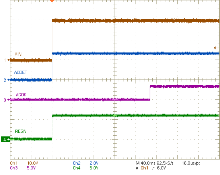
,
Figure 1. VCC, ACDET, REGN and ACOK Power Up | CH1: VCC, 10V/div, CH2: ACDET 2V/div, CH3: ACOK, 5V/div | ||
| CH4: REGN, 5V/div, 40ms/div |
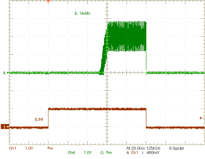
| CH1: ILIM, 1V/div | ||
| CH4: inductor current 1A/div, 20ms/div |
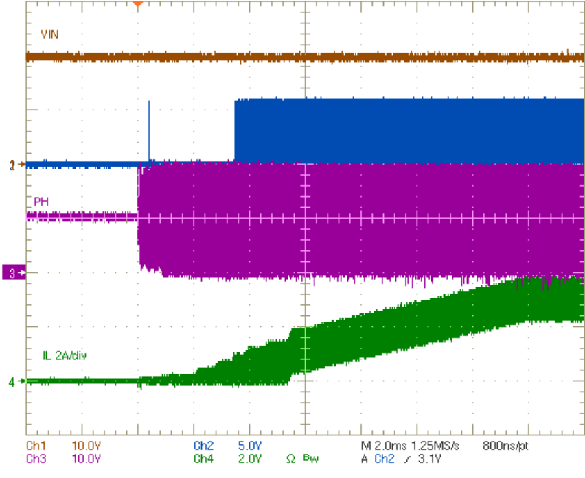
| CH1: Vin, 10V/div , CH2: LODRV, 5V/div, CH3: PHASE, 10V/div | ||
| CH4: inductor current, 2A/div, 2ms/div |
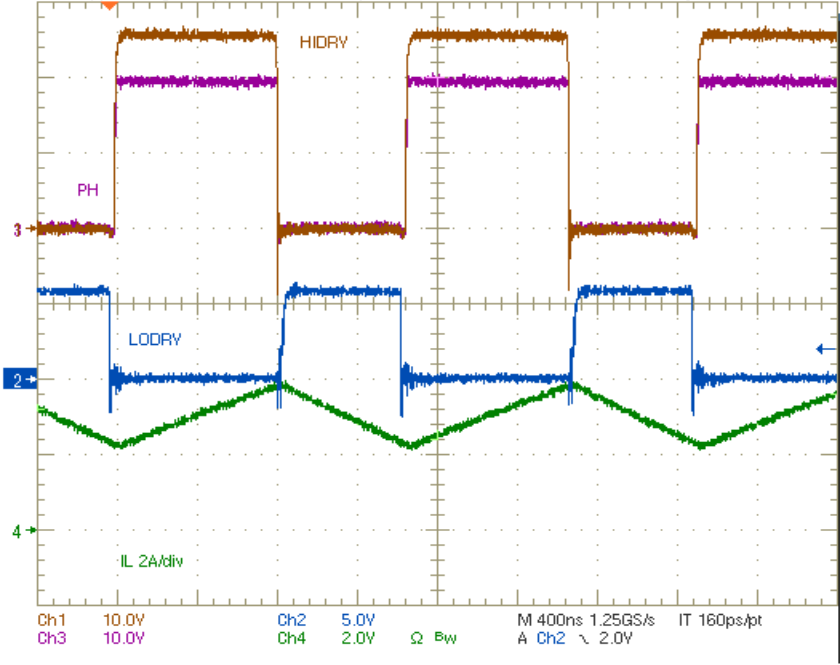
| CH1: PHASE, 10V/div, CH2: LODRV, 5V/div | ||
| CH3: HIDRV, 10V/div | ||
| CH4: inductor current, 2A/div, 400ns/div |
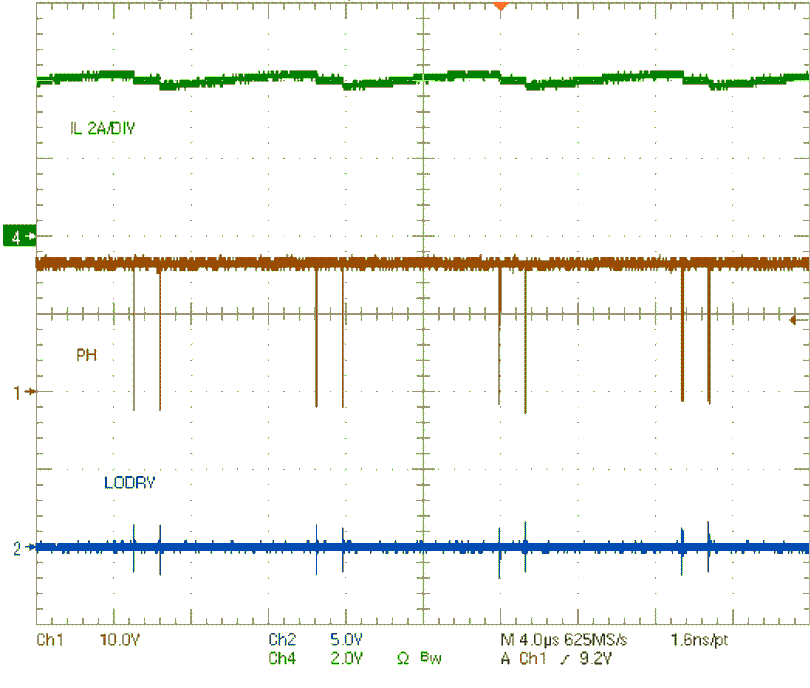
| CH1: PHASE, 10V/div, CH2: LODRV, 5V/div | ||
| CH4: inductor current, 2A/div, 4us/div |
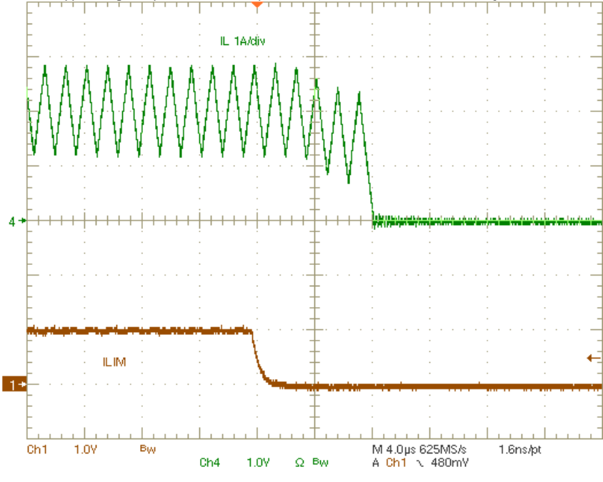
,
Figure 4. Charge Disable by ILIM | CH1: ILIM, 1V/div | ||
| CH4: inductor current, 1A/div, 4us/div |
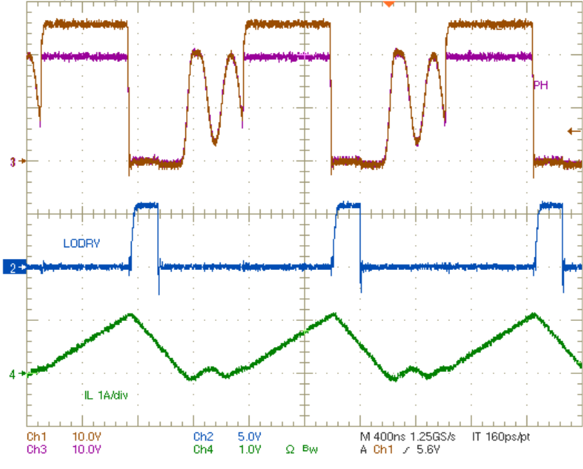
| CH1: PHASE, 10V/div, CH2: LODRV, 5V/div | ||
| CH3: HIDRV, 10V/div | ||
| CH4: inductor current, 1A/div, 400ns/div |
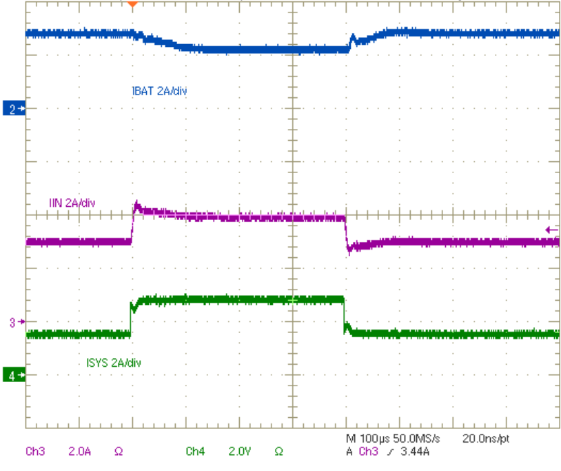
| CH2: battery current, 2A/div, CH3: adapter current, 2A/div | ||
| CH4: system load current, 2A/div, 100us/div |