SLUSCH6B March 2016 – March 2017
PRODUCTION DATA.
- 1 Features
- 2 Applications
- 3 Description
- 4 Revision History
- 5 Description (Continued)
- 6 Pin Configuration and Functions
- 7 Specifications
-
8 Detailed Description
- 8.1 Functional Block Diagram
- 8.2
Feature Description
- 8.2.1 Device Power-On-Reset (POR)
- 8.2.2 Device Power Up from Battery without Input Source
- 8.2.3 Device Power Up from Input Source
- 8.2.4 Power Path Management
- 8.2.5 Battery Charging Management
- 8.2.6 Battery Monitor
- 8.2.7 Status Outputs (PG, STAT, and INT)
- 8.2.8 Thermal Regulation and Thermal Shutdown
- 8.2.9 Voltage and Current Monitoring in Buck
- 8.2.10 Battery Protection
- 8.2.11 Serial Interface
- 8.3 Device Functional Modes
- 8.4 Register Map
- 9 Application and Implementation
- 10Power Supply Recommendations
- 11Layout
- 12Device and Documentation Support
- 13Mechanical, Packaging, and Orderable Information
1 Features
- Operation as Slave Charger to Provide Fast Charging in Dual Charger Operation
- Simple Configuration with Minimum BOM
- High Efficiency 3-A, 1.5-MHz Switch Mode Buck Charge
- 92% Charge Efficiency at 3 A and 94% Charge Efficiency at 2 A Charge Current
- Optimize for High Voltage Input (9 V / 12 V)
- Low Power PFM mode for Light Load Operations
- Single Input to Support USB Input and Adjustable High Voltage Adapters
- Support 3.9-V to 14-V Input Voltage Range
- Input Current Limit (100 mA to 3.25 A with 50-mA resolution) to Support USB2.0, USB3.0 standard and High Voltage Adapters
- Wide Input Dynamic Power Management (DPM) Range
- Highest Battery Discharge Efficiency with 5-mΩ Battery MOSFET
- Default Charge Disabled
- Integrated ADC for System Monitor
(Input, System and Battery Voltage, Temperature, Charge Current) - Flexible Autonomous and I2C Mode for Optimal System Performance
- Remote Battery Sensing
- High Integration includes all MOSFETs, Current Sensing and Loop Compensation
- High Accuracy
- ±0.5% Charge Voltage Regulation
- ±5% Charge Current Regulation
- ±7.5% Input Current Regulation
- Safety
- Thermal Regulation and Thermal Shutdown
- Input UVLO/Overvoltage Protection
- Battery OVP
- Safety Timer
2 Applications
- Smart Phone
- Tablet PC
- Portable Internet Devices
3 Description
The bq25898C is a highly-integrated switch-mode battery charge management and system power path management device for single cell Li-Ion and Li-polymer battery. The device supports high input voltage for charging. The low impedance power path optimizes switch-mode operation efficiency, reduces battery charging time and extends battery life during discharging phase. The I2C serial interface with charging and system settings makes the device a truly flexible solution. The bq25898C is available in a 2.8mm x 2.5mm 42-ball DSBGA package.
Device Information(1)
| PART NUMBER | PACKAGE | BODY SIZE (NOM) |
|---|---|---|
| bq25898C | DSBGA (42) | 2.80 mm x 2.50 mm |
- For all available packages, see the orderable addendum at the end of the data sheet.
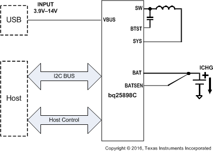
Simplified Schematic

4 Revision History
Changes from A Revision (December 2016) to B Revision
- Full data sheet to product folder Go
Changes from * Revision (March 2016) to A Revision
- Added Battery MOSFET to Highest Battery Discharge Efficiency FeatureGo
- Changed Integrated ADC for System Monitor Feature Go
- Changed charge disabled to both fast charge and precharge disabledGo
- Changed PG to PG in Description Go
- Changed anode to cathode in BTST Go
- Changed cathode to anode in REGN Go
- Deleted I(BOOST) from Electrical CharacteristicsGo
- Changed falling to rising in tACOV_RISING test conditions in Electrical CharacteristicsGo
- Changed 128 mA to 0 mA (precharge disabled) in Table 2 Go
- Changed 128 mA to 0 mA (precharge disabled) in Table 3 Go
- Changed Fast Charge Current from 4032 mA to 3008 mA in Figure 10Go
- Changed charge to both fast charge and precharge in Table 10 Go
- Changed 128mA (0001) to 0mA when REG04[5:0] = 000000 in Table 11Go
- Changed REG09 bits 5 - 2 from R/W to R Go
- Changed bit 5 in Table 15 Go
- Changed REG0B bit1 from x to 1 Go
- Added note to Figure 40 Go