JAJSEK1C August 2011 – August 2018 BUF20800-Q1
PRODUCTION DATA.
- 1 特長
- 2 アプリケーション
- 3 概要
- 4 改訂履歴
- 5 Pin Configuration and Functions
- 6 Specifications
- 7 Detailed Description
- 8 Application and Implementation
- 9 Power Supply Recommendations
- 10Layout
- 11デバイスおよびドキュメントのサポート
- 12メカニカル、パッケージ、および注文情報
パッケージ・オプション
メカニカル・データ(パッケージ|ピン)
- DCP|38
サーマルパッド・メカニカル・データ
- DCP|38
発注情報
7.1 Overview
The BUF20800-Q1 programmable voltage reference allows fast, easy adjustment of 18 programmable reference outputs and two channels for VCOM adjustment, each with 10-bit resolution. It offers very simple, time-efficient adjustment of the gamma reference and VCOM voltages. The BUF20800-Q1 is programmed through a high-speed, standard, two-wire interface. The BUF20800-Q1 features a double-register structure for each DAC channel to simplify the implementation of dynamic gamma control. This structure allows pre-loading of register data and rapid updating of all channels simultaneously.
Buffers 1−9 are able to swing to within 200mV of the positive supply rail, and to within 0.6V of the negative supply rail. Buffers 10−18 are able to swing to within 0.8V of the positive supply rail and to within 200mV of the negative supply rail.
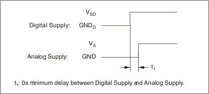
The BUF20800-Q1 can be powered using an analog supply voltage from 7V to 18V, and a digital supply from 2V to 5.5V. The digital supply must be applied prior to or simultaneously with the analog supply to avoid excessive current and power consumption; damage to the device may occur if it is left connected only to the analog supply for extended periods of time. Figure 7 shows the power supply timing requirements.
 Figure 7. Power Supply Timing Requirements
 Figure 14 shows the BUF20800-Q1 in a typical configuration. In this configuration, the BUF20800-Q1 device address is 74h. The output of each digital-to-analog converter (DAC) is immediately updated as soon as data are received in the corresponding register (LD = 0).
For maximum dynamic range, set VREFH = VS − 0.2 V and VREFL = GND + 0.2 V.