JAJSEK1C August 2011 – August 2018 BUF20800-Q1
PRODUCTION DATA.
- 1 特長
- 2 アプリケーション
- 3 概要
- 4 改訂履歴
- 5 Pin Configuration and Functions
- 6 Specifications
- 7 Detailed Description
- 8 Application and Implementation
- 9 Power Supply Recommendations
- 10Layout
- 11デバイスおよびドキュメントのサポート
- 12メカニカル、パッケージ、および注文情報
パッケージ・オプション
メカニカル・データ(パッケージ|ピン)
- DCP|38
サーマルパッド・メカニカル・データ
- DCP|38
発注情報
7.3.5 REFH and REFL Input range
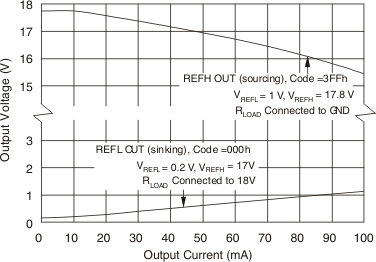
Best performance and output swing range of the BUF20800-Q1 are achieved by applying REFH and REFL voltages that are slightly below the power-supply voltages. Most specifications have been tested at REFH = Vs − 200mV and REFL = GND + 200mV. The REFH internal buffer is designed to swing very closely to Vs and the REFL internal buffer to GND. However, there is a finite limit on how close they can swing before saturating. To avoid saturation of the internal REFH and REFL buffers, the REFH voltage should not be greater than Vs −100mV and REFL voltage should not be lower than GND + 100mV. Figure 9 shows the swing capability of the REFH and REFL buffers.
The other consideration when trying to maximize the output swing capability of the gamma buffers is the limitation in the swing range of output buffers (OUT1−18, VCOM1, and VCOM2), which depends on the load current. A typical load in the LCD application is 5−10mA. For example, if OUT1 is sourcing 10mA, the swing is typically limited to about Vs − 200mV. The same applies to OUT18, which typically limits at GND + 200mV when sinking 10mA. An increase in output swing can only be achieved for much lighter loads. For example, a 3mA load typically allows the swing to be increased to approximately Vs − 100mV and GND + 100mV.
Connecting REFH directly to Vs and REFL directly to GND does not damage the BUF20800-Q1. As discussed above however, the output stages of the REFH and REFL buffers will saturate. This condition is not desirable and can result in a small error in the measured output voltages of OUT1−18, VCOM1, and VCOM2. As described above, this method of connecting REFH and REL does not help to maximize the output swing capability.
 Figure 9. Reference Buffer Output Voltage vs Output Current