SWRS111F June 2011 – October 2014 CC1121
PRODUCTION DATA.
- 1Device Overview
- 2Revision History
- 3Terminal Configuration and Functions
-
4Specifications
- 4.1 Absolute Maximum Ratings
- 4.2 Handling Ratings
- 4.3 Recommended Operating Conditions (General Characteristics)
- 4.4 Thermal Resistance Characteristics for RHB Package
- 4.5 RF Characteristics
- 4.6 Regulatory Standards
- 4.7 Current Consumption, Static Modes
- 4.8 Current Consumption, Transmit Modes
- 4.9 Current Consumption, Receive Modes
- 4.10
Receive Parameters
- 4.10.1 General Receive Parameters (High-Performance Mode)
- 4.10.2 RX Performance in 950-MHz Band (High-Performance Mode)
- 4.10.3 RX Performance in 868-, 915-, and 920-MHz Bands (High-Performance Mode)
- 4.10.4 RX Performance in 434-MHz Band (High-Performance Mode)
- 4.10.5 RX Performance in 169-MHz Band (High-Performance Mode)
- 4.10.6 RX Performance in Low-Power Mode
- 4.11 Transmit Parameters
- 4.12 PLL Parameters
- 4.13 Wake-up and Timing
- 4.14 32-MHz Crystal Oscillator
- 4.15 32-MHz Clock Input (TCXO) data to TCXO table
- 4.16 32-kHz Clock Input
- 4.17 32-kHz RC Oscillator
- 4.18 I/O and Reset
- 4.19 Temperature Sensor
- 4.20 Typical Characteristics
- 5Detailed Description
- 6Typical Application Circuit
- 7Device and Documentation Support
- 8Mechanical Packaging and Orderable Information
パッケージ・オプション
メカニカル・データ(パッケージ|ピン)
- RHB|32
サーマルパッド・メカニカル・データ
- RHB|32
発注情報
3 Terminal Configuration and Functions
3.1 Pin Diagram
Figure 3-1 shows pin names and locations for the CC1121 device.
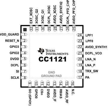 Figure 3-1 Package 5-mm × 5-mm QFN
3.2 Pin Configuration
The following table lists the pinout configuration for the CC1121 device.
| PIN NO. | PIN NAME | TYPE / DIRECTION | DESCRIPTION |
|---|---|---|---|
| 1 | VDD_GUARD | Power | 2.0–3.6 V VDD |
| 2 | RESET_N | Digital input | Asynchronous, active-low digital reset |
| 3 | GPIO3 | Digital I/O | General-purpose I/O |
| 4 | GPIO2 | Digital I/O | General-purpose I/O |
| 5 | DVDD | Power | 2.0–3.6 V VDD to internal digital regulator |
| 6 | DCPL | Power | Digital regulator output to external decoupling capacitor |
| 7 | SI | Digital input | Serial data in |
| 8 | SCLK | Digital input | Serial data clock |
| 9 | SO(GPIO1) | Digital I/O | Serial data out (general-purpose I/O) |
| 10 | GPIO0 | Digital I/O | General-purpose I/O |
| 11 | CSn | Digital Input | Active-low chip select |
| 12 | DVDD | Power | 2.0–3.6 V VDD |
| 13 | AVDD_IF | Power | 2.0–3.6 V VDD |
| 14 | RBIAS | Analog | External high-precision R |
| 15 | AVDD_RF | Power | 2.0–3.6 V VDD |
| 16 | N.C. | Not connected | |
| 17 | PA | Analog | Single-ended TX output (requires DC path to VDD) |
| 18 | TRX_SW | Analog | TX and RX switch. Connected internally to GND in TX and floating (high-impedance) in RX. |
| 19 | LNA_P | Analog | Differential RX input (requires DC path to GND) |
| 20 | LNA_N | Analog | Differential RX input (requires DC path to GND) |
| 21 | DCPL_VCO | Power | Pin for external decoupling of VCO supply regulator |
| 22 | AVDD_SYNTH1 | Power | 2.0–3.6 V VDD |
| 23 | LPF0 | Analog | External loop filter components |
| 24 | LPF1 | External loop filter components | |
| 25 | AVDD_PFD_CHP | Power | 2.0–3.6 V VDD |
| 26 | DCPL_PFD_CHP | Power | Pin for external decoupling of PFD and CHP regulator |
| 27 | AVDD_SYNTH2 | Power | 2.0–3.6 V VDD |
| 28 | AVDD_XOSC | Power | 2.0–3.6 V VDD |
| 29 | DCPL_XOSC | Power | Pin for external decoupling of XOSC supply regulator |
| 30 | XOSC_Q1 | Analog | Crystal oscillator pin 1 (must be grounded if a TCXO or other external clock connected to EXT_XOSC is used) |
| 31 | XOSC_Q2 | Analog | Crystal oscillator pin 2 (must be left floating if a TCXO or other external clock connected to EXT_XOSC is used) |
| 32 | EXT_XOSC | Digital input | Pin for external XOSC input (must be grounded if a regular XOSC connected to XOSC_Q1 and XOSC_Q2 is used) |
| – | GND | Ground pad | The ground pad must be connected to a solid ground plane. |