SWAS032F July 2013 – February 2015 CC3200
PRODUCTION DATA.
- 1Device Overview
- 2Revision History
- 3Terminal Configuration and Functions
-
4Specifications
- 4.1 Absolute Maximum Ratings
- 4.2 Handling Ratings
- 4.3 Power-On Hours
- 4.4 Recommended Operating Conditions
- 4.5 Brown-Out and Black-Out
- 4.6 Electrical Characteristics (3.3 V, 25°C)
- 4.7 WLAN Receiver Characteristics
- 4.8 WLAN Transmitter Characteristics
- 4.9 Current Consumption
- 4.10 Thermal Characteristics for RGC Package
- 4.11 Timing and Switching Characteristics
- 5Detailed Description
- 6Applications and Implementation
- 7Device and Documentation Support
- 8Mechanical Packaging and Orderable Information
パッケージ・オプション
メカニカル・データ(パッケージ|ピン)
- RGC|64
サーマルパッド・メカニカル・データ
- RGC|64
発注情報
3 Terminal Configuration and Functions
Figure 3-1 shows pin assignments for the 64-pin QFN package.
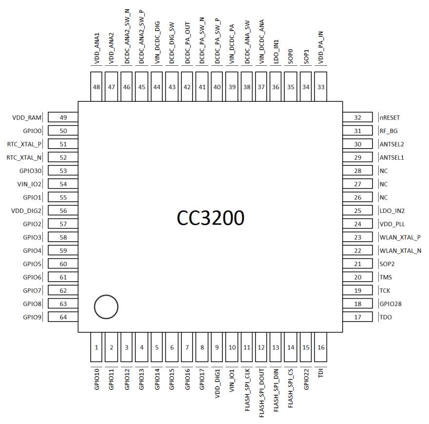 Figure 3-1 QFN 64-Pin Assignments (Top View)
3.1 Pin Attributes and Pin Multiplexing
The device makes extensive use of pin multiplexing to accommodate the large number of peripheral functions in the smallest possible package. To achieve this configuration, pin multiplexing is controlled using a combination of hardware configuration (at device reset) and register control.
NOTE
TI highly recommends using the CC3200 pin multiplexing utility to obtain the desired pinout.
The board and software designers are responsible for the proper pin multiplexing configuration. Hardware does not ensure that the proper pin multiplexing options are selected for the peripherals or interface mode used.
Table 3-1 describes the general pin attributes and presents an overview of pin multiplexing. All pin multiplexing options are configurable using the pin mux registers.
The following special considerations apply:
- All I/Os support drive strengths of 2, 4, and 6 mA. Drive strength is configurable individually for each pin.
- All I/Os support 10-µA pullups and pulldowns.
- These pulls are not active and all of the I/Os remain floating while the device is in Hibernate state.
- The VIO and VBAT supply must be tied together at all times.
- All digital I/Os are nonfail-safe.
NOTE
If an external device drives a positive voltage to the signal pads and the CC3200 device is not powered, DC current is drawn from the other device. If the drive strength of the external device is adequate, an unintentional wakeup and boot of the CC3200 device can occur. To prevent current draw, TI recommends any one of the following:
- All devices interfaced to the CC3200 device must be powered from the same power rail as the chip.
- Use level-shifters between the device and any external devices fed from other independent rails.
- The nRESET pin of the CC3200 device must be held low until the VBAT supply to the device is driven and stable.
Table 3-1 Pin Multiplexing
| General Pin Attributes | Function | Pad States | |||||||||||
|---|---|---|---|---|---|---|---|---|---|---|---|---|---|
| Pkg Pin | Pin Alias | Use | Select as Wakeup Source | Config Addl Analog Mux | Muxed with JTAG | Dig. Pin Mux Config Reg | Dig. Pin Mux Config Mode Value | Signal Name | Signal Description | Signal Direction | LPDS(1) | Hib(2) | nRESET = 0 |
| 1 | GPIO10 | I/O | No | No | No | GPIO_PAD_CONFIG_10 (0x4402 E0C8) |
0 | GPIO10 | General-Purpose I/O | I/O | Hi-Z | Hi-Z | Hi-Z |
| 1 | I2C_SCL | I2C Clock | O (Open Drain) |
Hi-Z | |||||||||
| 3 | GT_PWM06 | Pulse-Width Modulated O/P | O | Hi-Z | |||||||||
| 7 | UART1_TX | UART TX Data | O | 1 | |||||||||
| 6 | SDCARD_CLK | SD Card Clock | O | 0 | |||||||||
| 12 | GT_CCP01 | Timer Capture Port | I | Hi-Z | |||||||||
| 2 | GPIO11 | I/O | Yes | No | No | GPIO_PAD_CONFIG_11 (0x4402 E0CC) |
0 | GPIO11 | General-Purpose I/O | I/O | Hi-Z | Hi-Z | Hi-Z |
| 1 | I2C_SDA | I2C Data | I/O (Open Drain) |
Hi-Z | |||||||||
| 3 | GT_PWM07 | Pulse-Width Modulated O/P | O | Hi-Z | |||||||||
| 4 | pXCLK (XVCLK) | Free Clock To Parallel Camera | O | 0 | |||||||||
| 6 | SDCARD_CMD | SD Card Command Line | I/O | Hi-Z | |||||||||
| 7 | UART1_RX | UART RX Data | I | Hi-Z | |||||||||
| 12 | GT_CCP02 | Timer Capture Port | I | Hi-Z | |||||||||
| 13 | McAFSX | I2S Audio Port Frame Sync | O | Hi-Z | |||||||||
| 3 | GPIO12 | I/O | No | No | No | GPIO_PAD_CONFIG_12 (0x4402 E0D0) |
0 | GPIO12 | General Purpose I/O | I/O | Hi-Z | Hi-Z | Hi-Z |
| 3 | McACLK | I2S Audio Port Clock O | O | Hi-Z | |||||||||
| 4 | pVS (VSYNC) | Parallel Camera Vertical Sync | I | Hi-Z | |||||||||
| 5 | I2C_SCL | I2C Clock | I/O (Open Drain) |
Hi-Z | |||||||||
| 7 | UART0_TX | UART0 TX Data | O | 1 | |||||||||
| 12 | GT_CCP03 | Timer Capture Port | I | Hi-Z | |||||||||
| 4 | GPIO13 | I/O | Yes | No | No | GPIO_PAD_CONFIG_13 (0x4402 E0D4) |
0 | GPIO13 | General-Purpose I/O | I/O | Hi-Z | Hi-Z | Hi-Z |
| 5 | I2C_SDA | I2C Data | I/O (Open Drain) |
||||||||||
| 4 | pHS (HSYNC) | Parallel Camera Horizontal Sync | I | ||||||||||
| 7 | UART0_RX | UART0 RX Data | I | ||||||||||
| 12 | GT_CCP04 | Timer Capture Port | I | ||||||||||
| 5 | GPIO14 | I/O | No | No | GPIO_PAD_CONFIG_14 (0x4402 E0D8) |
0 | GPIO14 | General-Purpose I/O | I/O | Hi-Z | Hi-Z | Hi-Z | |
| 5 | I2C_SCL | I2C Clock | I/O (Open Drain) |
||||||||||
| 7 | GSPI_CLK | General SPI Clock | I/O | ||||||||||
| 4 | pDATA8 (CAM_D4) | Parallel Camera Data Bit 4 | I | ||||||||||
| 12 | GT_CCP05 | Timer Capture Port | I | ||||||||||
| 6 | GPIO15 | I/O | No | No | GPIO_PAD_CONFIG_15 (0x4402 E0DC) |
0 | GPIO15 | General-Purpose I/O | I/O | Hi-Z | Hi-Z | Hi-Z | |
| 5 | I2C_SDA | I2C Data | I/O (Open Drain) |
||||||||||
| 7 | GSPI_MISO | General SPI MISO | I/O | ||||||||||
| 4 | pDATA9 (CAM_D5) | Parallel Camera Data Bit 5 | I | ||||||||||
| 13 | GT_CCP06 | Timer Capture Port | I | ||||||||||
| 8 | SDCARD_ DATA0 |
SD Card Data | I/O | ||||||||||
| 7 | GPIO16 | I/O | No | No | GPIO_PAD_CONFIG_16 (0x4402 E0E0) |
0 | GPIO16 | General-Purpose I/O | I/O | Hi-Z | Hi-Z | Hi-Z | |
| Hi-Z | |||||||||||||
| Hi-Z | |||||||||||||
| 7 | GSPI_MOSI | General SPI MOSI | I/O | Hi-Z | |||||||||
| 4 | pDATA10 (CAM_D6) | Parallel Camera Data Bit 6 | I | Hi-Z | |||||||||
| 5 | UART1_TX | UART1 TX Data | O | 1 | |||||||||
| 13 | GT_CCP07 | Timer Capture Port | I | Hi-Z | |||||||||
| 8 | SDCARD_CLK | SD Card Clock | O | O | |||||||||
| 8 | GPIO17 | I/O | Wake-Up Source | No | No | GPIO_PAD_CONFIG_17 (0x4402 E0E4) |
0 | GPIO17 | General-Purpose I/O | I/O | Hi-Z | Hi-Z | Hi-Z |
| 5 | UART1_RX | UART1 RX Data | I | ||||||||||
| 7 | GSPI_CS | General SPI Chip Select | I/O | ||||||||||
| 4 | pDATA11 (CAM_D7) | Parallel Camera Data Bit 7 | I | ||||||||||
| 8 | SDCARD_ CMD |
SD Card Command Line | I/O | ||||||||||
| 9 | VDD_DIG1 | Int pwr | N/A | N/A | N/A | N/A | N/A | VDD_DIG1 | Internal Digital Core Voltage | ||||
| 10 | VIN_IO1 | Sup. input | N/A | N/A | N/A | N/A | N/A | VIN_IO1 | Chip Supply Voltage (VBAT) | ||||
| 11 | FLASH_SPI_ CLK |
O | N/A | N/A | N/A | N/A | N/A | FLASH_SPI_ CLK |
Clock To SPI Serial Flash (Fixed Default) | O | Hi-Z(3) | Hi-Z | Hi-Z |
| 12 | FLASH_SPI_DOUT | O | N/A | N/A | N/A | N/A | N/A | FLASH_SPI_ DOUT |
Data To SPI Serial Flash (Fixed Default) | O | Hi-Z(3) | Hi-Z | Hi-Z |
| 13 | FLASH_SPI_ DIN |
I | N/A | N/A | N/A | N/A | N/A | FLASH_SPI_ DIN |
Data From SPI Serial Flash (Fixed Default) | I | |||
| 14 | FLASH_SPI_ CS |
O | N/A | N/A | N/A | N/A | N/A | FLASH_SPI_ CS |
Chip Select To SPI Serial Flash (Fixed Default) | O | 1 | Hi-Z | Hi-Z |
| 15 | GPIO22 | I/O | No | No | No | GPIO_PAD_CONFIG_22 (0x4402 E0F8) |
0 | GPIO22 | General-Purpose I/O | I/O | Hi-Z | Hi-Z | Hi-Z |
| 7 | McAFSX | I2S Audio Port Frame Sync | O | Hi-Z | |||||||||
| 5 | GT_CCP04 | Timer Capture Port | I | ||||||||||
| 16 | TDI | I/O | No | No | MUXed with JTAG TDI | GPIO_PAD_CONFIG_23 (0x4402 E0FC) |
1 | TDI | JTAG TDI. Reset Default Pinout. | I | Hi-Z | Hi-Z | Hi-Z |
| 0 | GPIO23 | General-Purpose I/O | I/O | ||||||||||
| 2 | UART1_TX | UART1 TX Data | O | 1 | |||||||||
| 9 | I2C_SCL | I2C Clock | I/O (Open Drain) |
Hi-Z | |||||||||
| 17 | TDO | I/O | Wake-Up Source | No | MUXed with JTAG TDO | GPIO_PAD_CONFIG_ 24 (0x4402 E100) |
1 | TDO | JTAG TDO. Reset Default Pinout. | O | Hi-Z | Hi-Z | Hi-Z |
| 0 | GPIO24 | General-Purpose I/O | I/O | ||||||||||
| 5 | PWM0 | Pulse Width Modulated O/P | O | ||||||||||
| 2 | UART1_RX | UART1 RX Data | I | ||||||||||
| 9 | I2C_SDA | I2C Data | I/O (Open Drain) |
||||||||||
| 4 | GT_CCP06 | Timer Capture Port | I | ||||||||||
| 6 | McAFSX | I2S Audio Port Frame Sync | O | ||||||||||
| 18 | GPIO28 | I/O | No | GPIO_PAD_CONFIG_ 28 (0x4402 E110) |
0 | GPIO28 | General-Purpose I/O | I/O | Hi-Z | Hi-Z | Hi-Z | ||
| 19 | TCK | I/O | No | No | MUXed with JTAG/SWD-TCK | 1 | TCK | JTAG/SWD TCK Reset Default Pinout | I | Hi-Z | Hi-Z | Hi-Z | |
| 8 | GT_PWM03 | Pulse Width Modulated O/P | O | ||||||||||
| 20 | TMS | I/O | No | No | MUXed with JTAG/SWD-TMSC | GPIO_PAD_CONFIG_ 29 (0x4402 E114) |
1 | TMS | JATG/SWD TMS Reset Default Pinout | I/O | Hi-Z | Hi-Z | Hi-Z |
| 0 | GPIO29 | General-Purpose I/O | |||||||||||
| 21(4)(5) | SOP2 | O Only | No | No | No | GPIO_PAD_CONFIG_ 25 (0x4402 E104) |
0 | GPIO25 | General-Purpose I/O | O | Hi-Z | Driven Low | Hi-Z |
| 9 | GT_PWM02 | Pulse Width Modulated O/P | O | Hi-Z | |||||||||
| 2 | McAFSX | I2S Audio Port Frame Sync | O | Hi-Z | |||||||||
| See (6) | TCXO_EN | Enable to Optional External 40-MHz TCXO | O | O | |||||||||
| See (7) | SOP2 | Sense-On-Power 2 | I | ||||||||||
| 22 | WLAN_XTAL_N | WLAN Ana. | N/A | N/A | N/A | N/A | See (6) | WLAN_XTAL_N | 40-MHz XTAL Pulldown if ext TCXO is used. |
||||
| 23 | WLAN_XTAL_P | WLAN Ana. | N/A | N/A | N/A | N/A | WLAN_XTAL_P | 40-MHz XTAL or TCXO clock input | |||||
| 24 | VDD_PLL | Int. Pwr | N/A | N/A | N/A | N/A | VDD_PLL | Internal analog voltage | |||||
| 25 | LDO_IN2 | Int. Pwr | N/A | N/A | N/A | N/A | LDO_IN2 | Analog RF supply from ANA DC-DC output | |||||
| 26 | NC | WLAN Ana. | N/A | N/A | N/A | N/A | NC | Reserved | |||||
| 27 | NC | WLAN Ana. | N/A | N/A | N/A | N/A | NC | Reserved | |||||
| 28 | NC | WLAN Ana. | N/A | N/A | N/A | N/A | NC | Reserved | |||||
| 29(8) | ANTSEL1 | O Only | No | User config not required (9) |
No | GPIO_PAD_CONFIG_26 (0x4402 E108) |
0 | ANTSEL1(3) | Antenna Selection Control | O | Hi-Z | Hi-Z | Hi-Z |
| 30(8) | ANTSEL2 | O Only | No | User config not required (9) |
No | GPIO_PAD_CONFIG_27 (0x4402 E10C) |
0 | ANTSEL2(3) | Antenna Selection Control | O | Hi-Z | Hi-Z | Hi-Z |
| 31 | RF_BG | WLAN Ana. | N/A | N/A | N/A | N/A | RF_BG | RF BG band | |||||
| 32 | nRESET | Glob. Rst | N/A | N/A | N/A | N/A | nRESET | Master chip reset. Active low. | |||||
| 33 | VDD_PA_IN | Int. Pwr | N/A | N/A | N/A | N/A | VDD_PA_IN | PA supply voltage from PA DC-DC output. | |||||
| 34(5) | SOP1 | Config Sense | N/A | N/A | N/A | N/A | SOP1 | Sense On Power 1 | |||||
| 35(5) | SOP0 | Config Sense | N/A | N/A | N/A | N/A | SOP0 | Sense On Power 0 | |||||
| 36 | LDO_IN1 | Internal Power | N/A | N/A | N/A | N/A | LDO_IN1 | Analog RF supply from ana DC-DC output | |||||
| 37 | VIN_DCDC_ANA | Supply Input | N/A | N/A | N/A | N/A | VIN_DCDC_ ANA |
Analog DC-DC input (connected to chip input supply [VBAT]) | |||||
| 38 | DCDC_ANA_SW | Internal Power | N/A | N/A | N/A | N/A | DCDC_ANA_ SW |
Analog DC-DC switching node. | |||||
| 39 | VIN_DCDC_PA | Supply Input | N/A | N/A | N/A | N/A | VIN_DCDC_PA | PA DC-DC input (connected to chip input supply [VBAT]) | |||||
| 40 | DCDC_PA_SW_P | Internal Power | N/A | N/A | N/A | N/A | DCDC_PA_ SW_ P |
PA DCDC switching node | |||||
| 41 | DCDC_PA_SW_N | Internal Power | N/A | N/A | N/A | N/A | DCDC_PA_ SW_ N |
PA DCDC switching node | |||||
| 42 | DCDC_PA_OUT | Internal Power | N/A | N/A | N/A | N/A | DCDC_PA_ OUT |
PA buck converter output | |||||
| 43 | DCDC_DIG_SW | Internal Power | N/A | N/A | N/A | N/A | DCDC_DIG_ SW |
DIG DC-DC switching node | |||||
| 44 | VIN_DCDC_DIG | Supply Input | N/A | N/A | N/A | N/A | VIN_DCDC_ DIG |
DIG DC-DC input (connected to chip input supply [VBAT]) | |||||
| 45(10) | DCDC_ANA2_SW_P | I/O | No | User config not required (9)(11) |
No | GPIO_PAD_CONFIG_31 (0x4402 E11C) |
0 | GPIO31 | General-Purpose I/O | I/O | Hi-Z | Hi-Z | Hi-Z |
| 9 | UART0_RX | UART0 RX Data | I | ||||||||||
| 12 | McAFSX | I2S Audio Port Frame Sync | O | ||||||||||
| 2 | UART1_RX | UART1 RX Data | I | ||||||||||
| 6 | McAXR0 | I2S Audio Port Data 0 (RX/TX) | I/O | ||||||||||
| 7 | GSPI_CLK | General SPI Clock | I/O | ||||||||||
| See (6) | DCDC_ANA2_ SW_P |
ANA2 DCDC Converter +ve Switching Node. | |||||||||||
| 46 | DCDC_ANA2_SW_N | Internal Power | N/A | N/A | N/A | N/A | N/A | DCDC_ANA2_ SW_N |
ANA2 DCDC Converter -ve Switching Node. | ||||
| 47 | VDD_ANA2 | Internal Power | N/A | N/A | N/A | N/A | N/A | VDD_ANA2 | ANA2 DCDC O | ||||
| 48 | VDD_ANA1 | Internal Power | N/A | N/A | N/A | N/A | N/A | VDD_ANA1 | Analog supply fed by ANA2 DCDC output | ||||
| 49 | VDD_RAM | Internal Power | N/A | N/A | N/A | N/A | N/A | VDD_RAM | SRAM LDO output | ||||
| 50 | GPIO0 | I/O | No | User config not required (9) |
No | GPIO_PAD_CONFIG_0 (0x4402 E0A0) |
0 | GPIO0 | General-Purpose I/O | I/O | Hi-Z | Hi-Z | Hi-Z |
| 12 | UART0_CTS | UART0 Clear To Send Input (Active Low) | I | Hi-Z | Hi-Z | Hi-Z | |||||||
| 6 | McAXR1 | I2S Audio Port Data 1 (RX/TX) | I/O | Hi-Z | |||||||||
| 7 | GT_CCP00 | Timer Capture Port | I | Hi-Z | |||||||||
| 9 | GSPI_CS | General SPI Chip Select | I/O | Hi-Z | |||||||||
| 10 | UART1_RTS | UART1 Request To Send O (Active Low) | O | 1 | |||||||||
| 3 | UART0_RTS | UART0 Request To Send O (Active Low) | O | 1 | |||||||||
| 4 | McAXR0 | I2S Audio Port Data 0 (RX/TX) | I/O | Hi-Z | |||||||||
| 51 | RTC_XTAL_P | RTC Clock | N/A | N/A | N/A | N/A | RTC_XTAL_P | Connect 32.768-kHz XTAL or Froce external CMOS level clock | |||||
| 52(10) | RTC_XTAL_N | O Only | User config not required (9)(12) |
No | GPIO_PAD_CONFIG_32 (0x4402 E120) |
RTC_XTAL_N | Connect 32.768-kHz XTAL or connect a 100 kΩ to Vsupply. | Hi-Z | Hi-Z | ||||
| 0 | GPIO32 | General-Purpose I/O | I/O | Hi-Z | |||||||||
| 2 | McACLK | I2S Audio Port Clock O | O | Hi-Z | |||||||||
| 4 | McAXR0 | I2S Audio Port Data (Only O Mode Supported On Pin 52) | O | Hi-Z | |||||||||
| 6 | UART0_RTS | UART0 Request To Send O (Active Low) | O | 1 | |||||||||
| 8 | GSPI_MOSI | General SPI MOSI | I/O | Hi-Z | |||||||||
| 53 | GPIO30 | I/O | No | User config not required (9) |
No | GPIO_PAD_CONFIG_30 (0x4402 E118) |
0 | GPIO30 | General-Purpose I/O | I/O | Hi-Z | Hi-Z | Hi-Z |
| 9 | UART0_TX | UART0 TX Data | O | 1 | |||||||||
| 2 | McACLK | I2S Audio Port Clock O | O | Hi-Z | |||||||||
| 3 | McAFSX | I2S Audio Port Frame Sync | O | Hi-Z | |||||||||
| 4 | GT_CCP05 | Timer Capture Port | I | Hi-Z | |||||||||
| 7 | GSPI_MISO | General SPI MISO | I/O | Hi-Z | |||||||||
| 54 | VIN_IO2 | Supply Input | N/A | N/A | N/A | N/A | VIN_IO2 | Chip Supply Voltage (VBAT) | |||||
| 55 | GPIO1 | I/O | No | No | No | GPIO_PAD_CONFIG_1 (0x4402 E0A4) |
0 | GPIO1 | General-Purpose I/O | I/O | Hi-Z | Hi-Z | Hi-Z |
| 3 | UART0_TX | UART0 TX Data | O | 1 | |||||||||
| 4 | pCLK (PIXCLK) | Pixel Clock From Parallel Camera Sensor | I | Hi-Z | |||||||||
| 6 | UART1_TX | UART1 TX Data | O | 1 | |||||||||
| 7 | GT_CCP01 | Timer Capture Port | I | Hi-Z | |||||||||
| 56 | VDD_DIG2 | Internal Power | N/A | N/A | N/A | N/A | VDD_DIG2 | Internal Digital Core Voltage | |||||
| 57(13) | GPIO2 | Analog Input (up to 1.8 V)/ Digital I/O | Wake-Up Source | See (10)(14) | No | GPIO_PAD_CONFIG_2 (0x4402 E0A8) |
See (6) | ADC_CH0 | ADC Channel 0 Input (1.5V max) | I | Hi-Z | Hi-Z | |
| 0 | GPIO2 | General-Purpose I/O | I/O | Hi-Z | |||||||||
| 3 | UART0_RX | UART0 RX Data | I | Hi-Z | |||||||||
| 6 | UART1_RX | UART1 RXt Data | I | Hi-Z | |||||||||
| 7 | GT_CCP02 | Timer Capture Port | I | Hi-Z | |||||||||
| 58(13) | GPIO3 | Analog Input (up to 1.8 V)/ Digital I/O | No | See (10)(14) | No | GPIO_PAD_CONFIG_3 (0x4402 E0AC) |
See (6) | ADC_CH1 | ADC Channel 1 Input (1.5V max) | I | Hi-Z | Hi-Z | |
| 0 | GPIO3 | General-Purpose I/O | I/O | Hi-Z | |||||||||
| 6 | UART1_TX | UART1 TX Data | O | 1 | |||||||||
| 4 | pDATA7 (CAM_D3) | Parallel Camera Data Bit 3 | I | Hi-Z | |||||||||
| 59(13) | GPIO4 | Analog Input (up to 1.8 V)/ Digital I/O | Wake-up Source | See (10)(14) | No | GPIO_PAD_CONFIG_4 (0x4402 E0B0) |
See (6) | ADC_CH2 | ADC Channel 2 Input (1.5V max) | I | Hi-Z | Hi-Z | |
| 0 | GPIO4 | General-Purpose I/O | I/O | Hi-Z | |||||||||
| 6 | UART1_RX | UART1 RX Data | I | Hi-Z | |||||||||
| 4 | pDATA6 (CAM_D2) | Parallel Camera Data Bit 2 | I | Hi-Z | |||||||||
| 60(13) | GPIO5 | Analog Input (up to 1.8 V)/ Digital I/O | No | See (10)(14) | No | GPIO_PAD_CONFIG_5 (0x4402 E0B4) |
See (6) | ADC_CH3 | ADC Channel 3 Input (1.5V max) | I | Hi-Z | Hi-Z | |
| 0 | GPIO5 | General-Purpose I/O | I/O | Hi-Z | |||||||||
| 4 | pDATA5 (CAM_D1) | Parallel Camera Data Bit 1 | I | Hi-Z | |||||||||
| 6 | McAXR1 | I2S Audio Port Data 1 (RX/TX) | I/O | Hi-Z | |||||||||
| 7 | GT_CCP05 | Timer Capture Port | I | Hi-Z | |||||||||
| 61 | GPIO6 | I/O | No | No | No | GPIO_PAD_CONFIG_6 (0x4402 E0B8) |
0 | GPIO6 | General-Purpose I/O | I/O | Hi-Z | Hi-Z | Hi-Z |
| 5 | UART0_RTS | UART0 Request To Send O (Active Low) | O | 1 | |||||||||
| 4 | pDATA4 (CAM_D0) | Parallel Camera Data Bit 0 | I | Hi-Z | |||||||||
| 3 | UART1_CTS | UART1 Clear To Send Input (Active Low) | I | Hi-Z | |||||||||
| 6 | UART0_CTS | UART0 Clear To Send Input (Active Low) | I | Hi-Z | |||||||||
| 7 | GT_CCP06 | Timer Capture Port | I | Hi-Z | |||||||||
| 62 | GPIO7 | I/O | No | No | No | GPIO_PAD_CONFIG_7 (0x4402 E0BC) |
0 | GPIO7 | General-Purpose I/O | I/O | Hi-Z | Hi-Z | Hi-Z |
| 13 | McACLKX | I2S Audio Port Clock O | O | Hi-Z | |||||||||
| 3 | UART1_RTS | UART1 Request To Send O (Active Low) | O | 1 | |||||||||
| 10 | UART0_RTS | UART0 Request To Send O (Active Low) | O | 1 | |||||||||
| 11 | UART0_TX | UART0 TX Data | O | 1 | |||||||||
| 63 | GPIO8 | I/O | No | No | No | GPIO_PAD_CONFIG_8 (0x4402 E0C0) |
0 | GPIO8 | General-Purpose I/O | I/O | Hi-Z | Hi-Z | Hi-Z |
| 6 | SDCARD_IRQ | Interrupt from SD Card (Future support) | I | ||||||||||
| 7 | McAFSX | I2S Audio Port Frame Sync | O | ||||||||||
| 12 | GT_CCP06 | Timer Capture Port | I | ||||||||||
| 64 | GPIO9 | I/O | No | No | No | GPIO_PAD_CONFIG_9 (0x4402 E0C4) |
0 | GPIO9 | General-Purpose I/O | I/O | Hi-Z | Hi-Z | Hi-Z |
| 3 | GT_PWM05 | Pulse Width Modulated O/P | O | ||||||||||
| 6 | SDCARD_ DATA0 |
SD Cad Data | I/O | ||||||||||
| 7 | McAXR0 | I2S Audio Port Data (Rx/Tx) | I/O | ||||||||||
| 12 | GT_CCP00 | Timer Capture Port | I | ||||||||||
| 65 | GND_TAB | Thermal pad and electrical ground | |||||||||||
- LPDS mode: The state of unused GPIOs in LPDS is input with 500 kΩ pulldown. For all used GPIOs , the user can enable internal pulls, which would hold them in a valid state.
- Hibernate mode: The CC3200 device leaves the digital pins in a Hi-Z state without any internal pulls when the device enters hibernate state. This can cause glitches on output lines unless held at valid levels by external resistors.
- To minimize leakage in some serial flash vendors during LPDS, TI recommends the user application always enable internal weak pulldowns on FLASH_SPI_DATA and FLASH_SPI_CLK pins.
- This pin has dual functions: as a SOP[2] (device operation mode), and as an external TCXO enable. As a TXCO enable, the pin is an output on power up and driven logic high. During hibernate low-power mode, the pin is in a high impedance state but pulled down for SOP mode to disable TCXO. Because of SOP functionality, the pin must be used as output only.
- Higher leakage current from the onboard serial flash can occur due to floating inputs when the device enters Hibernate mode. See reference schematics for recommended pull-up and pull-down resistors.
- For details on proper use, see Section 3.2, Drive Strength and Reset States for Analog-Digital Multiplexed Pins.
- This pin is one of three that must have a passive pullup or pulldown resistor on board to configure the chip hardware power-up mode. For this reason, the pin must be output only when used for digital functions.
- This pin is reserved for WLAN antenna selection, controlling an external RF switch that multiplexes the RF pin of the CC3200 device between two antennas. These pins should not be used for other functionalities in general.
- Device firmware automatically enables the digital path during ROM boot.
- Pin 45 is used by an internal DC-DC (ANA2_DCDC) and pin 52 is used by the RTC XTAL oscillator. These modules use automatic configuration sensing. Therefore, some board-level configuration is required to use pin 45 and pin 52 as digital pads (see Figure 3-2). Because the CC3200R device does not require ANA2_DCDC, the pin can always be used for digital functions. However, pin 47 must be shorted to the supply input. Typically, pin 52 is used for RTC XTAL in most applications. However, in some applications a 32.768-kHz square-wave clock might always be available onboard. In such cases, the XTAL can be removed to free up pin 52 for digital functions. The external clock must then be applied at pin 51. For the chip to automatically detect this configuration, a 100K pull-up resistor must be connected between pin 52 and the supply line. To prevent false detection, TI recommends using pin 52 for output-only functions.
- VDD_FLASH must be shorted to Vsupply.
- To use the digital functions, RTC_XTAL_N must be pulled high to Vsupply using 100-KΩ resistor.
- This pin is shared by the ADC inputs and digital I/O pad cells. Important: The ADC inputs are tolerant up to 1.8 V. On the other hand, the digital pads can tolerate up to 3.6 V. Hence, care must be taken to prevent accidental damage to the ADC inputs. TI recommends that the output buffer(s) of the digital I/Os corresponding to the desired ADC channel be disabled first (that is, converted to high-impedance state), and thereafter the respective pass switches (S7, S8, S9, S10) should be enabled (see Section 3.2, Drive Strength and Reset States for Analog-Digital Multiplexed Pins).
- Requires user configuration to enable the ADC channel analog switch. (The switch is off by default.) The digital I/O is always connected and must be made Hi-Z before enabling the ADC switch.
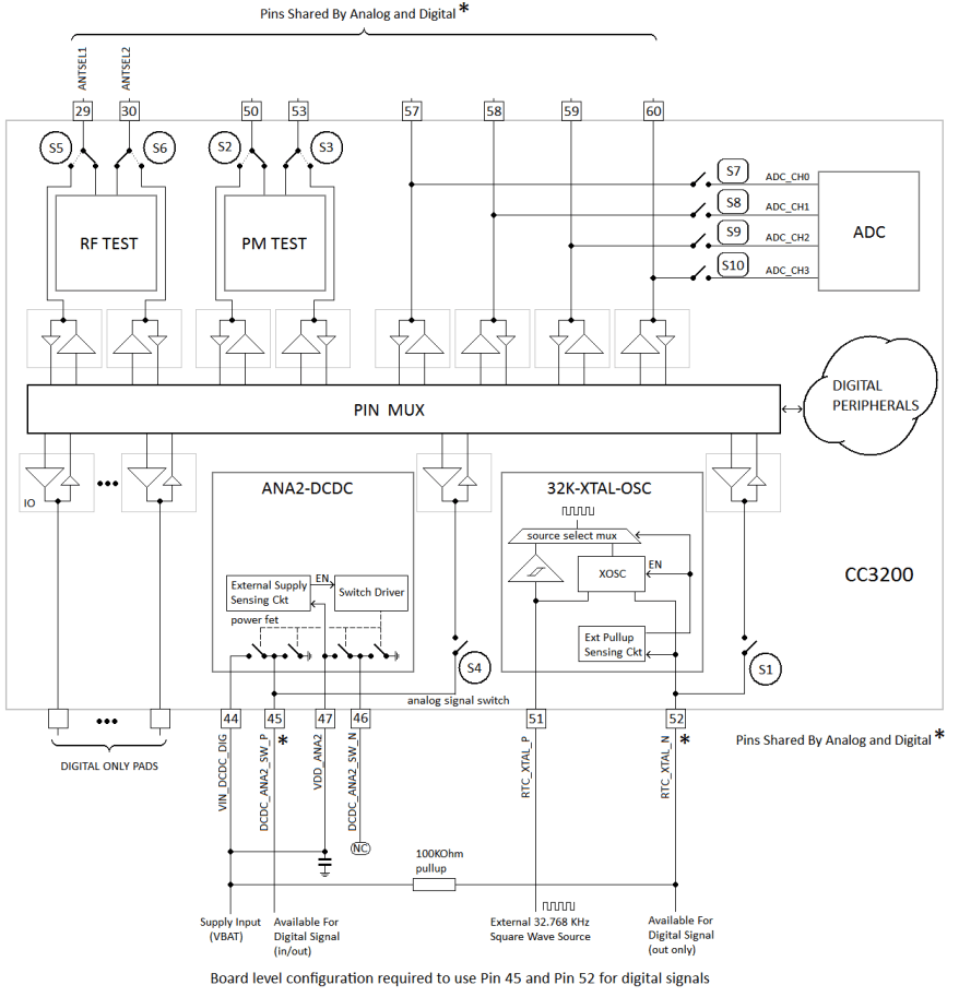 Figure 3-2 Board Configuration to Use Pins 45 and 52 as Digital Signals
3.1.1 Connections for Unused Pins
All unused pins must be left as no connect (NC) pins. For a list of NC pins, see Table 3-2.
Table 3-2 Connections for Unused Pins
| FUNCTION | SIGNAL NAME | PIN NUMBER |
|---|---|---|
| WLAN Analog | NC | 26 |
| WLAN Analog | NC | 27 |
| WLAN Analog | NC | 28 |
3.1.2 Recommended Pin Multiplexing Configurations
Table 3-3 lists the recommended pin multiplexing configurations.
Table 3-3 Recommended Pin Multiplexing Configurations
| CC3200 Recommended Pinout Grouping Use – Examples(2) | |||||||||||
|---|---|---|---|---|---|---|---|---|---|---|---|
| Home Security High-end Toys | Wifi Audio ++ Industrial | Sensor-Tag | Home Security Toys | Wifi Audio ++ Industrial | WiFi Remote w/ 7x7 keypad and audio | Sensor Door-Lock Fire-Alarm Toys w/o Cam | Industrial Home Appliances | Industrial Home Appliances Smart-Plug | Industrial Home Appliances" | GPIOs | |
| External 32 kHz(1) | External 32 kHz (1) | External TCXO 40 MHZ (-40 to +85°C) | |||||||||
| Cam + I2S (Tx or Rx) + I2C + SPI + SWD + UART-Tx + (App Logger) 2 GPIO + 1PWM + *4 overlaid wakeup from Hib | I2S (Tx & Rx) + 1 Ch ADC + 1x 4wire UART + 1x 2wire UART + 1bit SD Card + SPI + I2C + SWD + 3 GPIO + 1 PWM + 1 GPIO with Wake-From-Hib | I2S (Tx & Rx) + 2 Ch ADC + 2wire UART + SPI + I2C + SWD + 2 PMW + 6 GPIO + 3 GPIO with Wake-From-Hib | Cam + I2S (Tx or Rx) + I2C + SWD + UART-Tx + (App Logger) 4 GPIO + 1PWM + *4 overlaid wakeup from HIB | I2S (Tx & Rx) + 1 Ch ADC + 2x 2wire UART + 1bit SD Card + SPI + I2C + SWD + 4 GPIO + 1 PWM + 1 GPIO with Wake-From-Hib | I2S (Tx & Rx) + 1 Ch ADC + UART (Tx Only) I2C + SWD + 15 GPIO + 1 PWM + 1 GPIO with Wake-From-Hib | I2S (Tx or Rx) + 2 Ch ADC + 2 wire UART + SPI + I2C + 3 PMW + 3 GPIO with Wake-From-Hib + 5 GPIO SWD + | 4 Ch ADC + 1x 4wire UART + 1x 2wire UART + SPI + I2C + SWD + 1 PWM + 6 GPIO + 1 GPIO with Wake-From-Hib Enable for Ext 40 MHz TCXO | 3 Ch ADC + 2wire UART + SPI + I2C + SWD + 3 PWM + 9 GPIO + 2 GPIO with Wake-From-Hib | 2 Ch ADC + 2wire UART + I2C + SWD + 3 PWM + 11 GPIO + 5 GPIO with Wake-From-Hib | ||
| Pin Number | Pinout #11 | Pinout #10 | Pinout #9 | Pinout #8 | Pinout #7 | Pinout #6 | Pinout #5 | Pinout #4 | Pinout #3 | Pinout #2 | Pinout #1 |
| 52 | GSPI-MOSI | McASP-D0 (Tx) | GPIO_32 output only | ||||||||
| 53 | GSPI-MISO | MCASP-ACLKX | MCASP-ACLKX | GPIO_30 | GPIO_30 | GPIO_30 | GPIO_30 | UART0-TX | GPIO_30 | UART0-TX | GPIO_30 |
| 45 | GSPI-CLK | McASP-AFSX | McASP-D0 | GPIO_31 | McASP-AFSX | McASP-AFSX | McASP-AFSX | UART0-RX | GPIO_31 | UART0-RX | GPIO_31 |
| 50 | GSPI-CS | McASP-D1 (Rx) | McASP-D1 | McASP-D1 | McASP-D1 | McASP-D1 | McASP-D1 | UART0-CTS | GPIO_0 | GPIO_0 | GPIO_0 |
| 55 | pCLK (PIXCLK) | UART0-TX | UART0-TX | PIXCLK | UART0-TX | UART0-TX | UART0-TX | GPIO-1 | UART0-TX | GPIO_1 | GPIO_1 |
| 57 | (wake) GPIO2 | UART0-RX | UART0-RX | (wake) GPIO2 | UART0-RX | GPIO_2 | UART0-RX | ADC-0 | UART0-RX | (wake) GPIO_2 | (wake) GPIO_2 |
| 58 | pDATA7 (D3) | UART1-TX | ADC-CH1 | pDATA7 (D3) | UART1-TX | GPIO_3 | ADC-1 | ADC-1 | ADC-1 | ADC-1 | GPIO_3 |
| 59 | pDATA6 (D2) | UART1-RX | (wake) GPIO_4 | pDATA6 (D2) | UART1-RX | GPIO_4 | (wake) GPIO_4 | ADC-2 | ADC-2 | (wake) GPIO_4 | (wake) GPIO_4 |
| 60 | pDATA5 (D1) | ADC-3 | ADC-3 | pDATA5 (D1) | ADC-3 | ADC-3 | ADC-3 | ADC-3 | ADC-3 | ADC-3 | GPIO_5 |
| 61 | pDATA4 (D0) | UART1-CTS | GPIO_6 | pDATA4 (D0) | GPIO_6 | GPIO_6 | GPIO_6 | UART0-RTS | GPIO_6 | GPIO_6 | GPIO_6 |
| 62 | McASP-ACLKX | UART1-RTS | GPIO_7 | McASP-ACLKX | McASP-ACLKX | McASP-ACLKX | McASP-ACLKX | GPIO_7 | GPIO_7 | GPIO_7 | GPIO_7 |
| 63 | McASP-AFSX | SDCARD-IRQ | McASP-AFSX | McASP-AFSX | SDCARD-IRQ | GPIO_8 | GPIO_8 | GPIO_8 | GPIO_8 | GPIO_8 | GPIO_8 |
| 64 | McASP-D0 | SDCARD-DATA | GT_PWM5 | McASP-D0 | SDCARD-DATA | GPIO_9 | GT_PWM5 | GT_PWM5 | GT_PWM5 | GT_PWM5 | GPIO_9 |
| 1 | UART1-TX | SDCARD-CLK | GPIO_10 | UART1-TX | SDCARD-CLK | GPIO_10 | GT_PWM6 | UART1-TX | GT_PWM6 | GPIO_10 | GPIO_10 |
| 2 | (wake) pXCLK (XVCLK) | SDCARD-CMD | (wake) GPIO_11 | (wake) pXCLK (XVCLK) | SDCARD-CMD | GPIO_11 | (wake) GPIO_11 | UART1-RX | (wake) GPIO_11 | (wake) GPIO_11 | (wake) GPIO_11 |
| 3 | pVS (VSYNC) | I2C-SCL | I2C-SCL | pVS (VSYNC) | I2C-SCL | GPIO_12 | I2C-SCL | I2C-SCL | I2C-SCL | GPIO_12 | GPIO_12 |
| 4 | (wake) pHS (HSYNC) | I2C-SDA | I2C-SDA | (wake) pHS (HSYNC) | I2C-SDA | GPIO_13 | I2C-SDA | I2C-SDA | I2C-SDA | (wake) GPIO_13 | (wake) GPIO_13 |
| 5 | pDATA8 (D4) | GSPI-CLK | GSPI-CLK | pDATA8 (D4) | GSPI-CLK | I2C-SCL | GSPI-CLK | GSPI-CLK | GSPI-CLK | I2C-SCL | GPIO_14 |
| 6 | pDATA9 (D5) | GSPI-MISO | GSPI-MISO | pDATA9 (D5) | GSPI-MISO | I2C-SDA | GSPI-MISO | GSPI-MISO | GSPI-MISO | I2C-SDA | GPIO_15 |
| 7 | pDATA10 (D6) | GSPI-MOSI | GSPI-MOSI | pDATA10 (D6) | GSPI-MOSI | GPIO_16 | GSPI-MOSI | GSPI-MOSI | GSPI-MOSI | GPIO_16 | GPIO_16 |
| 8 | (wake) pDATA11 (D7) | GSPI-CS | GSPI-CS | (wake) pDATA11 (D7) | GSPI-CS | GPIO_17 | GSPI-CS | GSPI-CS | GSPI-CS | (wake) GPIO_17 | (wake) GPIO_17 |
| 11 | SPI-FLASH_CLK | SPI-FLASH_CLK | SPI-FLASH_CLK | SPI-FLASH_CLK | SPI-FLASH_CLK | SPI-FLASH_CLK | SPI-FLASH_CLK | SPI-FLASH_CLK | SPI-FLASH_CLK | SPI-FLASH_CLK | SPI-FLASH_CLK |
| 12 | SPI-FLASH-DOUT | SPI-FLASH-DOUT | SPI-FLASH-DOUT | SPI-FLASH-DOUT | SPI-FLASH-DOUT | SPI-FLASH-DOUT | SPI-FLASH-DOUT | SPI-FLASH-DOUT | SPI-FLASH-DOUT | SPI-FLASH-DOUT | SPI-FLASH-DOUT |
| 13 | SPI-FLASH-DIN | SPI-FLASH-DIN | SPI-FLASH-DIN | SPI-FLASH-DIN | SPI-FLASH-DIN | SPI-FLASH-DIN | SPI-FLASH-DIN | SPI-FLASH-DIN | SPI-FLASH-DIN | SPI-FLASH-DIN | SPI-FLASH-DIN |
| 14 | SPI-FLASH-CS | SPI-FLASH-CS | SPI-FLASH-CS | SPI-FLASH-CS | SPI-FLASH-CS | SPI-FLASH-CS | SPI-FLASH-CS | SPI-FLASH-CS | SPI-FLASH-CS | SPI-FLASH-CS | SPI-FLASH-CS |
| 15 | GPIO_22 | GPIO_22 | GPIO_22 | GPIO_22 | GPIO_22 | GPIO_22 | GPIO_22 | GPIO_22 | GPIO_22 | GPIO_22 | GPIO_22 |
| 16 | I2C-SCL | GPIO_23 | GPIO_23 | I2C-SCL | GPIO_23 | GPIO_23 | GPIO_23 | GPIO_23 | GPIO_23 | GPIO_23 | GPIO_23 |
| 17 | I2C-SDA | (wake) GPIO_24 | (wake) GPIO_24 | I2C-SDA | (wake) GPIO_24 | (wake) GPIO_24 | (wake) GPIO_24 | (wake) GPIO_24 | (wake) GPIO_24 | GT-PWM0 | (wake) GPIO_24 |
| 19 | SWD-TCK | SWD-TCK | SWD-TCK | SWD-TCK | SWD-TCK | SWD-TCK | SWD-TCK | SWD-TCK | SWD-TCK | SWD-TCK | SWD-TCK |
| 20 | SWD-TMS | SWD-TMS | SWD-TMS | SWD-TMS | SWD-TMS | SWD-TMS | SWD-TMS | SWD-TMS | SWD-TMS | SWD-TMS | SWD-TMS |
| 18 | GPIO_28 | GPIO_28 | GPIO_28 | GPIO_28 | GPIO_28 | GPIO_28 | GPIO_28 | GPIO_28 | GPIO_28 | GPIO_28 | GPIO_28 |
| 21 | GT_PWM2 | GT_PWM2 | GT_PWM2 | GT_PWM2 | GT_PWM2 | GT_PWM2 | GT_PWM2 | TCXO_EN | GT_PWM2 | GT_PWM2 | GPIO_25 out only |
3.2 Drive Strength and Reset States for Analog-Digital Multiplexed Pins
Table 3-4 describes the use, drive strength, and default state of these pins at first-time power up and reset (nRESET pulled low).
Table 3-4 Drive Strength and Reset States for Analog-Digital Multiplexed Pins
| Pin | Board Level Configuration and Use | Default State at First Power Up or Forced Reset | State after Configuration of Analog Switches (ACTIVE, LPDS, and HIB Power Modes) | Maximum Effective Drive Strength (mA) |
|---|---|---|---|---|
| 29 | Connected to the enable pin of the RF switch (ANTSEL1). Other use not recommended. | Analog is isolated. The digital I/O cell is also isolated. | Determined by the I/O state, as are other digital I/Os. | 4 |
| 30 | Connected to the enable pin of the RF switch (ANTSEL2). Other use not recommended. | Analog is isolated. The digital I/O cell is also isolated. | Determined by the I/O state, as are other digital I/Os. | 4 |
| 45 | VDD_ANA2 (pin 47) must be shorted to the input supply rail. Otherwise, the pin is driven by the ANA2 DC-DC. | Analog is isolated. The digital I/O cell is also isolated. | Determined by the I/O state, as are other digital I/Os. | 4 |
| 50 | Generic I/O | Analog is isolated. The digital I/O cell is also isolated. | Determined by the I/O state, as are other digital I/Os. | 4 |
| 52 | The pin must have an external pullup of 100 K to the supply rail and must be used in output signals only. | Analog is isolated. The digital I/O cell is also isolated. | Determined by the I/O state, as are other digital I/Os. | 4 |
| 53 | Generic I/O | Analog is isolated. The digital I/O cell is also isolated. | Determined by the I/O state, as are other digital I/Os. | 4 |
| 57 | Analog signal (1.8 V absolute, 1.46 V full scale) | ADC is isolated. The digital I/O cell is also isolated. | Determined by the I/O state, as are other digital I/Os. | 4 |
| 58 | Analog signal (1.8 V absolute, 1.46 V full scale) | ADC is isolated. The digital I/O cell is also isolated. | Determined by the I/O state, as are other digital I/Os. | 4 |
| 59 | Analog signal (1.8 V absolute, 1.46 V full scale) | ADC is isolated. The digital I/O cell is also isolated. | Determined by the I/O state, as are other digital I/Os. | 4 |
| 60 | Analog signal (1.8 V absolute, 1.46 V full scale) | ADC is isolated. The digital I/O cell is also isolated. | Determined by the I/O state, as are other digital I/Os. | 4 |
3.3 Pad State After Application of Power To Chip But Prior To Reset Release
When a stable power is applied to the CC3200 chip for the first time or when supply voltage is restored to the proper value following a prior period with supply voltage below 1.5 V, the level of the digital pads are undefined in the period starting from the release of nRESET and until DIG_DCDC powers up. This period is less than approximately 10 ms. During this period, pads can be internally pulled weakly in either direction. If a certain set of pins are required to have a definite value during this pre-reset period, an appropriate pullup or pulldown must be used at the board level. The recommended value of this external pull is 2.7 KΩ.