JAJSFA6F July 2013 – February 2022 CSD17483F4
PRODUCTION DATA
- 1特長
- 2アプリケーション
- 3概要
- 4Revision History
- 5Specifications
- 6Device and Documentation Support
- 7Mechanical, Packaging, and Orderable Information
パッケージ・オプション
デバイスごとのパッケージ図は、PDF版データシートをご参照ください。
メカニカル・データ(パッケージ|ピン)
- YJC|3
サーマルパッド・メカニカル・データ
発注情報
5.3 Typical MOSFET Characteristics
TA = 25°C (unless otherwise stated)
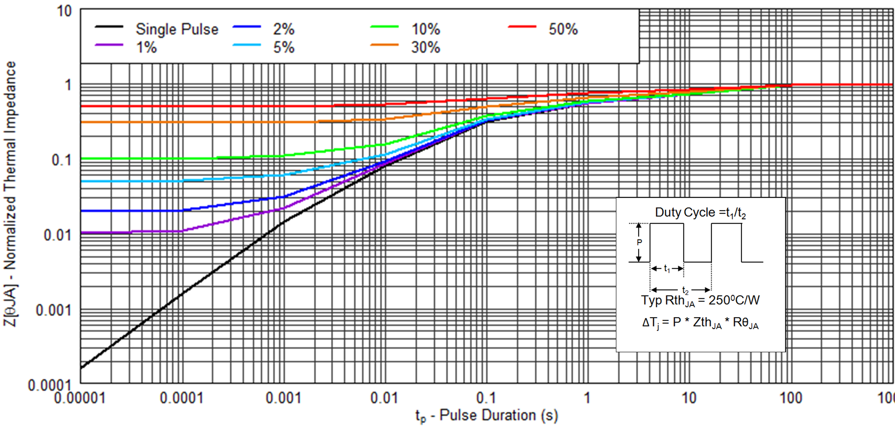 Figure 5-1 Transient
Thermal Impedance
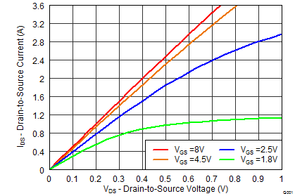 Figure 5-2 Saturation Characteristics
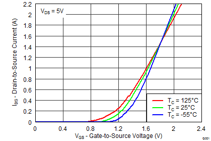 Figure 5-3 Transfer Characteristics
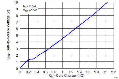 Figure 5-4 Gate Charge
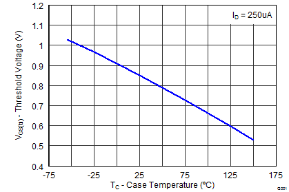 Figure 5-6 Threshold Voltage vs Temperature
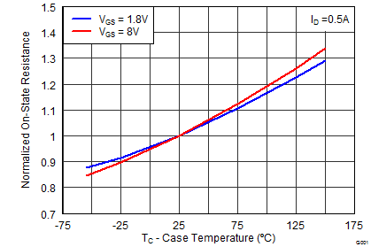 Figure 5-8 Normalized On-State Resistance vs Temperature
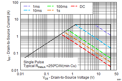 Figure 5-10 Maximum Safe Operating Area
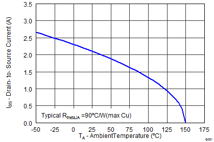 Figure 5-12 Maximum Drain Current vs Temperature
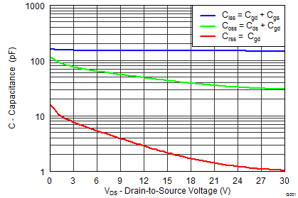 Figure 5-5 Capacitance
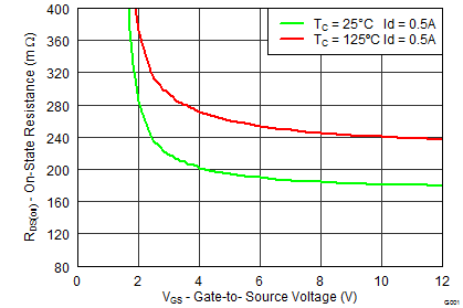 Figure 5-7 On-State Resistance vs Gate-to-Source Voltage
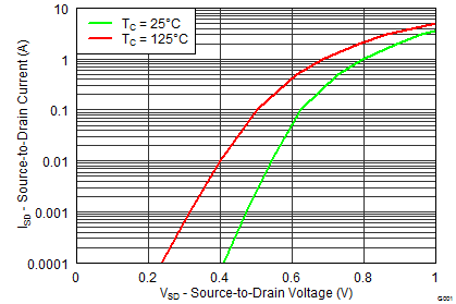 Figure 5-9 Typical Diode Forward Voltage
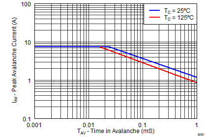 Figure 5-11 Single Pulse Unclamped Inductive Switching