SLPS393A October 2013 – January 2015 CSD17571Q2
PRODUCTION DATA.
- 1Features
- 2Applications
- 3Description
- 4Revision History
- 5 Specifications
- 6Device and Documentation Support
- 7Mechanical, Packaging, and Orderable Information
パッケージ・オプション
デバイスごとのパッケージ図は、PDF版データシートをご参照ください。
メカニカル・データ(パッケージ|ピン)
- DQK|6
サーマルパッド・メカニカル・データ
発注情報
1 Features
- Low Qg and Qgd
- Low Thermal Resistance
- Avalanche Rated
- Pb-Free Terminal Plating
- RoHS Compliant
- Halogen Free
- SON 2 mm × 2 mm Plastic Package
2 Applications
- Optimized for Load Switch Applications
- Storage, Tablets, and Handheld Devices
- Optimized for Control FET Applications
3 Description
This 30 V, 20 mΩ, SON 2×2 NexFET™ power MOSFET is designed to minimize losses in power conversion and load management applications, while offering excellent thermal performance for the size of the package.
Top View
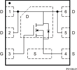
Product Summary
| TA = 25°C | TYPICAL VALUE | UNIT | ||
|---|---|---|---|---|
| VDS | Drain-to-Source Voltage | 30 | V | |
| Qg | Gate Charge Total (4.5 V) | 2.4 | nC | |
| Qgd | Gate Charge Gate-to-Drain | 0.6 | nC | |
| RDS(on) | Drain-to-Source On-Resistance | VGS = 4.5 V | 24 | mΩ |
| VGS = 10 V | 20 | mΩ | ||
| VGS(th) | Threshold Voltage | 1.6 | V | |
Ordering Information(1)
| Device | Media | Qty | Package | Ship |
|---|---|---|---|---|
| CSD17571Q2 | 7-Inch Reel | 3000 | SON 2 x 2 mm Plastic Package | Tape and Reel |
- For all available packages, see the orderable addendum at the end of the data sheet.
Absolute Maximum Ratings
| TA = 25°C | VALUE | UNIT | |
|---|---|---|---|
| VDS | Drain-to-Source Voltage | 30 | V |
| VGS | Gate-to-Source Voltage | ±20 | V |
| ID | Continuous Drain Current (Package Limit) | 22 | A |
| Continuous Drain Current(1) | 7.6 | A | |
| IDM | Pulsed Drain Current, TA = 25°C(2) | 39 | A |
| PD | Power Dissipation(1) | 2.5 | W |
| TJ, Tstg |
Operating Junction and Storage Temperature Range |
–55 to 150 | °C |
| EAS | Avalanche Energy, single pulse ID = 12 A, L = 0.1 mH, RG = 25 Ω |
7.2 | mJ |
- RθJA = 50 on 1 in² Cu (2 oz.) on 0.060" thick FR4 PCB
- Pulse duration 10 μs, duty cycle ≤2%
RDS(on) vs VGS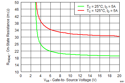 |
Gate Charge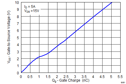 |