SLASE16B January 2014 – May 2014 DAC37J82 , DAC38J82
PRODUCTION DATA.
- 1 Features
- 2 Applications
- 3 Description
- 4 Revision History
- 5 Pin Configuration and Functions
-
6 Specifications
- 6.1 Absolute Maximum Ratings
- 6.2 Handling Ratings
- 6.3 Recommended Operating Conditions
- 6.4 Thermal Information
- 6.5 DC Electrical Characteristics
- 6.6 Digital Electrical Characteristics
- 6.7 AC Electrical Characteristics
- 6.8 Timing Requirements
- 6.9 Switching Characteristics
- 6.10 Typical Characteristics
-
7 Detailed Description
- 7.1 Overview
- 7.2 Functional Block Diagram
- 7.3
Feature Description
- 7.3.1 Serdes Input
- 7.3.2 Serdes Rate
- 7.3.3 Serdes PLL
- 7.3.4 Serdes Equalizer
- 7.3.5 JESD204B Descrambler
- 7.3.6 JESD204B Frame Assembly
- 7.3.7 Serial Peripheral Interface (SPI)
- 7.3.8 Multi-Device Synchronization
- 7.3.9 Input Multiplexer
- 7.3.10 FIR Filters
- 7.3.11 Full Complex Mixer
- 7.3.12 Coarse Mixer
- 7.3.13 Dithering
- 7.3.14 Complex Summation
- 7.3.15 Quadrature Modulation Correction (QMC)
- 7.3.16 Group Delay Correction Block
- 7.3.17 Output Multiplexer
- 7.3.18 Power Measurement And Power Amplifier Protection
- 7.3.19 Serdes Test Modes
- 7.3.20 Error Counter
- 7.3.21 Eye Scan
- 7.3.22 JESD204B Pattern Test
- 7.3.23 Temperature Sensor
- 7.3.24 Alarm Monitoring
- 7.3.25 LVPECL Inputs
- 7.3.26 CMOS Digital Inputs
- 7.3.27 Reference Operation
- 7.3.28 Analog Outputs
- 7.3.29 DAC Transfer Function
- 7.4 Device Functional Modes
- 7.5 Register Map
- 8 Applications and Implementation
- 9 Power Supply Recommendations
- 10Layout
- 11Device and Documentation Support
- 12Mechanical, Packaging, and Orderable Information
1 Features
- Resolution: 16-Bit
- Maximum Sample Rate:
- DAC37J82: 1.6 GSPS
- DAC38J82: 2.5 GSPS
- Maximum Input Data Rate: 1.23GSPS
- JESD204B Interface
- 8 JESD204B Serial Input Lanes
- 12.5 Gbps Maximum Bit Rate per Lane
- Subclass 1 Multi-DAC synchronization
- On-Chip Very Low Jitter PLL
- Selectable 1x -16x Interpolation
- Independent Complex Mixers with 48-bit NCO/ or ±n×Fs/8
- Wideband Digital Quadrature Modulator Correction
- Sinx/x Correction Filters
- Fractional Sample Group Delay Correction
- Flexible Routing to Four Analog Outputs via Output Multiplexer
- 3/4-Wire Serial Control Bus (SPI)
- Integrated Temperature Sensor
- JTAG Boundary Scan
- Pin-compatible with Quad-channel DAC37J84/DAC38J84
- Power Dissipation: 1.1W at 2.5GSPS
- Package: 10x10mm, 144-Ball Flip-Chip BGA
2 Applications
- Cellular Base Stations
- Diversity Transmit
- Wideband Communications
- Direct Digital Synthesis (DDS) Instruments
- Millimeter/Microwave Backhaul
- Automated Test Equipment
- Cable Infrastructure
- Radar
3 Description
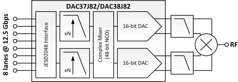
The pin-compatible DAC37J82/DAC38J82 family is a very low power, 16-bit, dual-channel, 1.6/2.5 GSPS digital to analog converter (DAC) with JESD204B interface. The maximum input data rate is 1.23 GSPS.
Digital data is input to the device through 1, 2, 4 or 8 configurable serial JESD204B lanes running up to 12.5 Gbps with on-chip termination and programmable equalization. The interface allows JESD204B Subclass 1 SYSREF based deterministic latency and full synchronization of multiple devices.
The device includes features that simplify the design of complex transmit architectures. Fully bypassable 2x to 16x digital interpolation filters with over 90 dB of stop-band attenuation simplify the data interface and reconstruction filters. An on-chip 48-bit Numerically Controlled Oscillator (NCO) and independent complex mixers allow flexible and accurate carrier placement.
A high-performance low jitter PLL simplifies clocking of the device without significant impact on the dynamic range. The digital Quadrature Modulator Correction (QMC) and Group Delay Correction (QDC) enable complete IQ compensation for gain, offset, phase, and group delay between channels in direct up-conversion applications. A programmable Power Amplifier (PA) protection mechanism is available to provide PA protection in cases when the abnormal power behavior of the input data is detected.
DAC37J82/DAC38J82 family provides four analog outputs, and the data from the internal two digital paths can be routed to any two out of these four DAC outputs via the output multiplexer.
Device Information(1)
| PART NUMBER | PACKAGE | BODY SIZE (NOM) |
|---|---|---|
| DAC37J82 | FCBGA (144) | 10.00 mm x 10.00 mm |
| DAC38J82 | FCBGA (144) | 10.00 mm x 10.00 mm |
- For all available packages, see the orderable addendum at the end of the datasheet.